CRYSTALLINE SILICON SURFACE PASSIVATION BY THE
advertisement
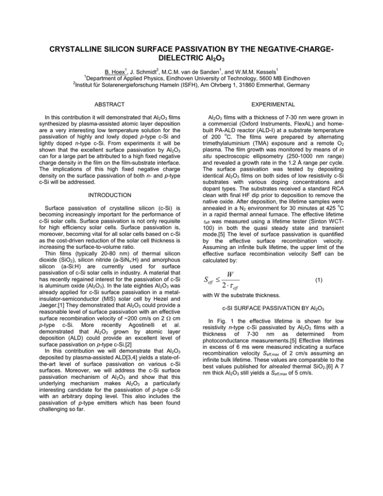
CRYSTALLINE SILICON SURFACE PASSIVATION BY THE NEGATIVE-CHARGEDIELECTRIC Al2O3 1 2 1 1 B. Hoex , J. Schmidt , M.C.M. van de Sanden , and W.M.M. Kessels Department of Applied Physics, Eindhoven University of Technology, 5600 MB Eindhoven 2 Institut für Solarenergieforschung Hameln (ISFH), Am Ohrberg 1, 31860 Emmerthal, Germany 1 ABSTRACT EXPERIMENTAL In this contribution it will demonstrated that Al2O3 films synthesized by plasma-assisted atomic layer deposition are a very interesting low temperature solution for the passivation of highly and lowly doped p-type c-Si and lightly doped n-type c-Si. From experiments it will be shown that the excellent surface passivation by Al2O3 can for a large part be attributed to a high fixed negative charge density in the film on the film-substrate interface. The implications of this high fixed negative charge density on the surface passivation of both n- and p-type c-Si will be addressed. Al2O3 films with a thickness of 7-30 nm were grown in a commercial (Oxford Instruments, FlexAL) and homebuilt PA-ALD reactor (ALD-I) at a substrate temperature o of 200 C. The films were prepared by alternating trimethylaluminium (TMA) exposure and a remote O2 plasma. The film growth was monitored by means of in situ spectroscopic ellipsometry (250-1000 nm range) and revealed a growth rate in the 1.2 Å range per cycle. The surface passivation was tested by depositing identical Al2O3 films on both sides of low resistivity c-Si substrates with various doping concentrations and dopant types. The substrates received a standard RCA clean with final HF dip prior to deposition to remove the native oxide. After deposition, the lifetime samples were o annealed in a N2 environment for 30 minutes at 425 C in a rapid thermal anneal furnace. The effective lifetime τeff was measured using a lifetime tester (Sinton WCT100) in both the quasi steady state and transient mode.[5] The level of surface passivation is quantified by the effective surface recombination velocity. Assuming an infinite bulk lifetime, the upper limit of the effective surface recombination velocity Seff can be calculated by: INTRODUCTION Surface passivation of crystalline silicon (c-Si) is becoming increasingly important for the performance of c-Si solar cells. Surface passivation is not only requisite for high efficiency solar cells. Surface passivation is, moreover, becoming vital for all solar cells based on c-Si as the cost-driven reduction of the solar cell thickness is increasing the surface-to-volume ratio. Thin films (typically 20-80 nm) of thermal silicon dioxide (SiO2), silicon nitride (a-SiNx:H) and amorphous silicon (a-Si:H) are currently used for surface passivation of c-Si solar cells in industry. A material that has recently regained interest for the passivation of c-Si is aluminum oxide (Al2O3). In the late eighties Al2O3 was already applied for c-Si surface passivation in a metalinsulator-semiconductor (MIS) solar cell by Hezel and Jaeger.[1] They demonstrated that Al2O3 could provide a reasonable level of surface passivation with an effective surface recombination velocity of ~200 cm/s on 2 Ω cm p-type c-Si. More recently Agostinelli et al. demonstrated that Al2O3 grown by atomic layer deposition (ALD) could provide an excellent level of surface passivation on p-type c-Si.[2] In this contribution we will demonstrate that Al2O3 deposited by plasma-assisted ALD[3,4] yields a state-ofthe-art level of surface passivation on various c-Si surfaces. Moreover, we will address the c-Si surface passivation mechanism of Al2O3 and show that this underlying mechanism makes Al2O3 a particularly interesting candidate for the passivation of p-type c-Si with an arbitrary doping level. This also includes the passivation of p-type emitters which has been found challenging so far. Seff ≤ W 2 ⋅τ eff (1) with W the substrate thickness. c-SI SURFACE PASSIVATION BY Al2O3 In Fig. 1 the effective lifetime is shown for low resistivity n-type c-Si passivated by Al2O3 films with a thickness of 7-30 nm as determined from photoconductance measurements.[5] Effective lifetimes in excess of 6 ms were measured indicating a surface recombination velocity Seff,max of 2 cm/s assuming an infinite bulk lifetime. These values are comparable to the best values published for alnealed thermal SiO2.[6] A 7 nm thick Al2O3 still yields a Seff,max of 5 cm/s. Figure 3 clearly demonstrates that Al2O3 provides a state-the-art level of surface passivation on p-type c-Si with an arbitrary doping level. The excellent level of surface passivation by Al2O3 was also confirmed by solar cell device performance. Al2O3 applied at the rear of p-type c-Si solar cells yielded a maximum efficiency of 20.6 %. This work was done in collaboration with the solar cell institute ISFH in Germany and will be presented in a separate contribution at this conference.[11,12] The performance of the Al2O3 passivated solar cells was at least equal to the solar cells with an alnealed thermal SiO2 rear surface passivation.[11,12] -2 Effective lifetime (s) 10 -3 10 26 nm 13 nm 7 nm -4 10 12 10 10 13 10 14 15 10 10 16 17 10 -3 Injection level ∆n (cm ) c-Si SURFACE PASSIVATION MECHANISM OF Al2O3 Figure 1: Effective lifetime as a function of the excess carrier density for low resistivity n-type (275 µm, <100>, 1.9 Ω cm) float zone c-Si substrate passivated with a 30, 15 and 7 nm thick Al2O3 film.[7] In Fig. 2 the effective lifetime is shown for a 2 Ω cm ptype wafer passivated by a 10 and 30 nm Al2O3 film. Effective lifetimes in excess of 3 ms were measured, corresponding to a Seff,max of 5 cm/s. In Fig. 3 the combined Seff, max values are shown for p-type c-Si with various doping concentrations passivated by Al2O3. Literature values obtained by thermal SiO2 (either forming gas annealed or alnealed), as deposited aSiNx:H and a-Si:H are included for comparison. The 18 -3 values for a B-doping concentration > 10 cm were extracted from the measured emitter saturation current density on B-doped p-type emitters as discussed in detail in a separate publication.[8] The effective surface recombination values for lightly B-doped c-Si were calculated assuming an infinite bulk lifetime and using the best values published in the studies of Kerr et al. [6,9,10] and Dauwe et al.[9] In Fig. 4 field-effect passivation is simulated for a moderately doped n-type c-Si wafer for both a negative and positive charge density Qeffective at the surface. It can clearly be seen that a high positive or negative Qeffective results in a significant reduction of Seff. For a sufficiently high Qeffective the minority surface carrier density scales 2 with 1/Q at the c-Si surface; hence the field-effect 2 passivation scales with Q , irrespective of the polarity of the Qeffective. The surface passivation mechanism of Al2O3 is mainly based on field-effect passivation by a high fixed negative charge density Qf in the Al2O3 film. In Fig. 5 it is demonstrated that a positive corona charge density 13 -2 Qcorona of 1.3×10 cm at the Al2O3 surface is required to cancel the field effect passivation. Qcorona is balancing the negative fixed charge density in a 26 nm Al2O3 film, resulting in a maximum in Seff. Negative fixed charges are routinely reported for Al2O3 films deposited on c-Si, irrespective of the deposition technique. The origin of these negative charges is most probably related to the 6 10 -2 10 Al2O3 5 Seff, max (cm/s) Effective lifetime (s) 10 -3 10 Thermal SiO2 as-deposited a-SiNx:H 4 10 a-Si:H 3 10 2 10 1 10 0 -4 10 13 10 10 14 10 15 10 16 17 10 -3 10 15 10 10 16 10 17 10 18 10 19 -3 Surface B-density (cm ) Injection level (cm ) Figure 2: Effective lifetime as a function of the excess carrier density for low resistivity p-type (300 µm, <111>, 2 Ω cm) float zone c-Si substrate passivated with a 30 and 10 nm thick Al2O3 film. Figure 3: Upper level of the effective surface recombination velocity as a function of the Bconcentration for c-Si wafers passivated by plasmaassisted ALD Al2O3, thermal SiO2, a-SiNx:H, and aSi:H.[6,9,10] 4 1000 10 Qf in 26 nm Al2O3 film 13 -1.3×10 cm 3 10 -2 100 Seff (cm/s) Normalized Seff 1.9 Ω cm n-type 2 10 1/Q 1 2 2 1/Q effective effective 10 10 Qeffective positive Qeffective negative 1 0 10 -10 -5 0 5 12 10 0 5 10 15 12 -2 20 -2 Qcorona (10 cm ) Qeffective (10 cm ) Figure 4: Normalized Seff for a 1.9 Ω cm n-type c-Si surface as a function of the fixed charge density Qeffective present at the surface. These simulations were performed in PC1D.[13] Figure 5: Seff of a n-type c-Si (1.9 Ω cm <100> 275 µm) wafer symmetrically passivated by a 26 nm Al2O3 film as a function of the positive corona charge density deposited at the surface. presence of Al vacancies in the Al2O3 film.[14] It was shown that these vacancies are predominantly present at the c-Si/Al2O3 interface,[15] in excellent agreement with the position of the fixed negative charge density deduced from thickness dependent capacitance voltage measurements by for example Abouaf et al.[16] A negative Qf is especially beneficial for the passivation of p-type c-Si as the minority carriers, the electrons, are effectively shielded from the c-Si surface. This is clearly apparent from the fact that the negativecharge-dielectric Al2O3 provides a state-of-the-art level of surface passivation even on highly B-doped p-type cSi surfaces as shown in Fig. 3. The negative sign of the fixed charge also explains the flat injection level dependence of the surface passivation on low resistivity p-type c-Si as shown in Fig. 2 of this proceeding in excellent agreement with the extended Shockley-ReadHall model.[17] A strong injection level dependence is routinely reported for p-type c-Si passivated by thermal SiO2, a-SiNx:H and a-Si:H.[6,9,10] As the fixed charge density in Al2O3 is typically one order of magnitude higher compared to a-SiNx:H and two orders of magnitude higher compared to thermal SiO2 and a-SiCx this implies that the field-effect passivation by Al2O3 is 2 - 4 orders of magnitude stronger compared to these types of surface passivation films. This difference in the level of field-effect passivation significantly relaxes the requirements on the interface defect density at the cSi/Al2O3 interface. However, the relative low Seff at the point where the field-effect passivation is cancelled in Fig. 5 illustrates that the c-Si/Al2O3 interface defect density is also relatively low due to the presence of a thin SiO2-like film between the c-Si and the Al2O3 film as generated during the Al2O3 deposition process.[7] CONCLUSIONS It is demonstrated that Al2O3 is an interesting material to obtain a high level of c-Si surface passivation as required for high efficiency solar cells. Al2O3 not only yields a state-of-the-art level of surface passivation on low resistivity n- and p-type c-Si, but its high fixed negative charge density makes it also particularly interesting for the passivation of p-type c-Si with an arbitrary doping level such as highly doped p-type emitters. The field-effect passivation by Al2O3 is orders of magnitude stronger than for passivation layers such as a-SiNx:H and thermal SiO2 and this relaxes the demanding requirements on the electrical interface quality. The excellent level of surface passivation has already been demonstrated by p-type c-Si solar cell devices. ACKNOWLEDGMENTS The authors thank W. Keuning (Eindhoven University of Technology) and all members of the photovoltaic department at ISFH for their contributions to this work REFERENCES [1] [2] [3] [4] R. Hezel and K. Jaeger, J. Electrochem. Soc. 136, 518 (1989). G. Agostinelli, A. Delabie, P. Vitanov, Z. Alexieva, H. F. W. Dekkers, S. De Wolf, and G. Beaucarne, Sol. Energ. Mat. Sol. C. 90, 3438 (2006). J.L. van Hemmen, S. B. S. Heil, J. Klootwijk, F. Roozeboom, C.J. Hodson, M. C. M. van de Sanden, and W. M. M. Kessels, J. Electrochem. Soc. 154, G165 (2007). W. M. M. Kessels, B. Hoex, and M. C. M. van de Sanden, This conference. [5] [6] [7] [8] [9] [10] [11] [12] [13] [14] [15] [16] [17] R. A. Sinton and A. Cuevas, Appl. Phys. Lett. 69, 2510 (1996). M. J. Kerr and A. Cuevas, Semicond. Sci. Tech. 17, 35 (2002). B. Hoex, S. B. S. Heil, E. Langereis, M. C. M. van de Sanden, and W. M. M. Kessels, Appl. Phys. Lett. 89, 042112 (2006). B. Hoex, J. Schmidt, R. Bock, P. P. Altermatt, M. C. M. van de Sanden, and W. M. M. Kessels, Appl. Phys. Lett. 91, 112107 (2007). S. Dauwe, J. Schmidt, and R. Hezel, Proc. of the 29th IEEE Photovoltaic Specialist Conference, New Orleans, (IEEE, Piscataway, NJ, 2002), p. 1246. M. J. Kerr and A. Cuevas, Semicond. Sci. Tech. 17, 166 (2002). J. Schmidt, A. Merkle, R. Brendel, B. Hoex, M. C. M. van de Sanden, and W. M. M. Kessels, This conference. J. Schmidt, A. Merkle, R. Brendel, B. Hoex, M. C. M. van de Sanden, and W. M. M. Kessels, Progr. Photovoltaics, 10.1002/pip.823 (2008). P. A. Basore, IEEE Trans. Electron. Dev. 37, 337 (1990). K. Matsunaga, T. Tanaka, T. Yamamoto, and Y. Ikuhara, Phys. Rev. B 68, 085110 (2003). K. Kimoto, Y. Matsui, T. Nabatame, T. Yasuda, T. Mizoguchi, I. Tanaka, and A. Toriumi, Appl. Phys. Lett. 83, 4306 (2003). J. A. Aboaf, D. R. Kerr, and E. Bassous, J. Electrochem. Soc. 120, 1103 (1973). R. B. M. Girisch, R. P. Mertens, and R. F. Dekeersmaecker, IEEE Trans. Electron Devices 35, 203 (1988).
