AN1681/D How to Keep a FLYBACK Switch Mode Supply
advertisement
AN1681/D
How to Keep a FLYBACK
Switch Mode Supply Stable
with a Critical-Mode
Controller
http://onsemi.com
Prepared by: Christophe BASSO, MOTOROLA SPS
BP-1029, Le Mirail,
31023 Toulouse France
email: R38010@email.sps.mot.com;
Tel.: 33 5 61 19 90 12
APPLICATION NOTE
INTRODUCTION
Defining the Mode
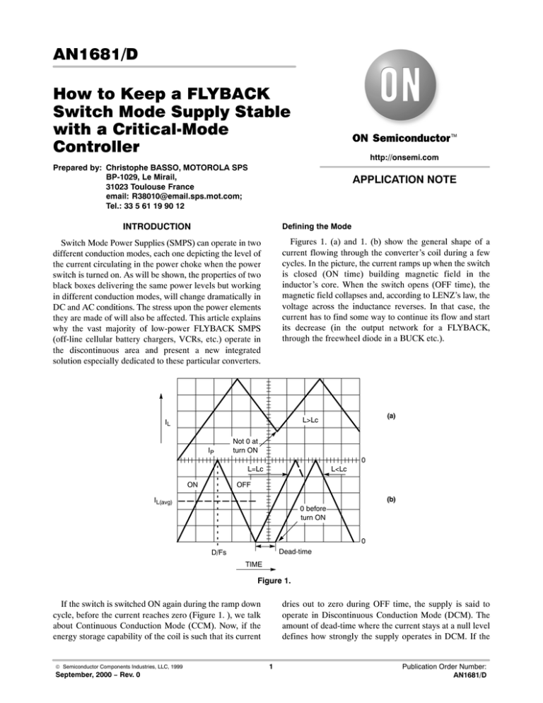
Figures 1. (a) and 1. (b) show the general shape of a
current flowing through the converter’s coil during a few
cycles. In the picture, the current ramps up when the switch
is closed (ON time) building magnetic field in the
inductor’s core. When the switch opens (OFF time), the
magnetic field collapses and, according to LENZ’s law, the
voltage across the inductance reverses. In that case, the
current has to find some way to continue its flow and start
its decrease (in the output network for a FLYBACK,
through the freewheel diode in a BUCK etc.).
Switch Mode Power Supplies (SMPS) can operate in two
different conduction modes, each one depicting the level of
the current circulating in the power choke when the power
switch is turned on. As will be shown, the properties of two
black boxes delivering the same power levels but working
in different conduction modes, will change dramatically in
DC and AC conditions. The stress upon the power elements
they are made of will also be affected. This article explains
why the vast majority of low-power FLYBACK SMPS
(off-line cellular battery chargers, VCRs, etc.) operate in
the discontinuous area and present a new integrated
solution especially dedicated to these particular converters.
(a)
L>Lc
IL
IP
Not 0 at
turn ON
0
L=Lc
ON
L<Lc
OFF
(b)
IL(avg)
0 before
turn ON
0
Dead-time
D/Fs
TIME
Figure 1.
If the switch is switched ON again during the ramp down
cycle, before the current reaches zero (Figure 1. ), we talk
about Continuous Conduction Mode (CCM). Now, if the
energy storage capability of the coil is such that its current
© Semiconductor Components Industries, LLC, 1999
September, 2000 − Rev. 0
dries out to zero during OFF time, the supply is said to
operate in Discontinuous Conduction Mode (DCM). The
amount of dead-time where the current stays at a null level
defines how strongly the supply operates in DCM. If the
1
Publication Order Number:
AN1681/D
AN1681/D
deals with a known inductance L. What level of load, RC,
will push my supply into CCM? Or what minimum load my
SMPS should see before entering DCM? The third one uses
fixed values of the above elements but adjusts the operating
frequency, FC, to stay in critical conduction. These
questions can be answered after a few lines of algebra
corresponding to Figure 2. ’s example, a FLYBACK
converter:
current through the coil reaches zero and the switch turns
ON immediately (no dead-time), the converter operates in
Critical Conduction Mode.
Where is the Boundary?
There are three ways you can think of the boundary
between the modes. One is about the critical value of the
inductance, LC, for which the supply will work in either
CCM or DCM given a fixed nominal load. The second
ÉÉ
ÉÉÉÉÉÉ
ÉÉÉÉ
1:N
5
Lp
+
VDD
4
2
VDD.N
Rload
Ls
1
3
DT
PWM
Vo
(1-D)T
Voltage across the
secondary coil
(b)
(a)
Figure 2.
To help determine some key characteristics of this
converter, we will refer to the following statements:
• The average inductor voltage per cycle should be null (1)
• From Figure 1. (b), when L=LC, IL(avg) = Ip/2 (2)
• A 100% efficiency leads to Pin=Pout (3)
The DC voltage transfer ratio in CCM is first determined
using statement (1), thus equating Figure 2. (b)’s areas:
If we introduce these elements in the above equations, we
can solve for the critical values of RC, LC and FC:
R
L
V
@ N @ D + Vo @ (1 * D).
DD
Vout
D
+
@ N (4).
(1 * D)
V
in
V @ dt + L @ dI thus,
L
L
•
•
+
R @ (1 * D) 2
C
2 @ Fs @ N 2
+
R @ (1 * D) 2
C
2 @ L @ N2
C
The FLYBACK converter, as with the BOOST and
BUCK-BOOST structures, has an operating mode
comparable to someone filling a bucket (coil) with water
and flushing it into a water tank (capacitor). The bucket is
first presented to the spring (ON time) until its inner level
reaches a defined limit. Then the bucket is removed from
the spring (OFF time) and flushed into a water tank that
supplies a fire engine (load). The bucket can be totally
emptied before refilling (DCM) or some water can remain
before the user presents it back to the spring (CCM). Let’s
suppose that the man is experimented and he ensures that
the recurrence period (ON+OFF time) is constant. The
end-user is a fireman who closes the feedback loop via his
voice, shouting for more or less flow for the tank. Now, if
the flames suddenly get bigger, the fireman will require
more power from its engine and will ask the bucket man to
provide the tank with a higher flow. In other words, the
bucket operator will fill his container longer (ON time
Ip
ŕ VL @ dt + Lc @ ŕ dIL.
0
C
2 @ L @ Fs @ N 2
C
(1 * D) 2
Filling-in the Bucket
As we can see from Figure 1. (b), the flux stored in the
coil during the ON time is down to zero right at the
beginning of the next cycle when the inductance equals its
critical value (L=LC ). Mathematically this can be
expressed by integrating the formula:
•
C
F
After factorization, it comes
D
Fs
C
+
0
V @D
å in
+ L @ Ip + 2 @ I
@ L , from (2).
L(avg)
C
C
Fs
From (3), Vin @ I L(avg) + I o @ (Vin @ N ) Vout), or
V
I
+ I o @ (N ) out)
L(avg)
V
in
Vout
By definition, I o +
and Vout + Vin @ N @ D
1*D
R
from (4).
http://onsemi.com
2
AN1681/D
increases). BUT, since by experience he keeps his working
period constant, the time he will spend in flushing into the
tank will naturally diminish (OFF time decreases), so will
the amount of water poured. The fire engine will run out of
power, making the fireman shout louder for more water,
extending the filling time etc. The loop oscillates! This
behavior is typical for converters in which the energy
transfer is not direct (unlike the BUCK derived families)
and severely affects the overall dynamic performances. In
time domain, a large step load increase requires a
corresponding percentage rise of the inductor current. This
necessitates a temporary duty-cycle augmentation which
(with only two operational states) causes the diode
conduction time to diminish. Therefore, it implies a
decrease in the average diode current at first, rather than an
increase as desired. When heavily into the continuous mode
and if the inductor current rate is small compared to the
current level, it can take many cycles for the inductor
current to reach the new value. During this time, the output
current is actually reduced because the diode conduction
time (TOFF) has been decreased, even if the peak diode
current is rising. In DCM, by definition, a third state is
present whether neither the diode or the switch conduct and
the inductor current is null. This « idle time» allows the
switch duty cycle to lengthen in presence of a step load
increase without lowering the diode conduction time. In
fact, it is possible for the DCM circuit to adapt perfectly to
a step load change of any magnitude in the very first
switching period, with the switch conduction time, the peak
current, and the diode conduction time all increasing at
once to the values that will be maintained forevermore at
the new load current.
The extra delay is mathematically described by a Right
Half-Plane Zero (RHPZ) in the transfer function
(Av +
and forces the designer to roll-off the loop gain at a point
where the phase margin is still secure. Actually, a classical
zero in the Left Half-Plane
(Av +
(1 ) S z1) @ AAA
)
AAA
provides a boost in gain AND phase at the point it is
inserted. Unfortunately, the RHPZ gives a boost in gain, but
lags the phase. More viciously, its position moves as a
function of the load which makes its compensation an
almost impossible exercise. Rolling-off the gain well under
the worse RHPZ position is the usual solution. Let’s also
point out that the low-frequency RHPZ is only present in
FLYBACK type converters (BOOST, BUCK-BOOST)
operating in CCM and moves to higher-frequencies (then
becoming negligible) when the power supply enters DCM.
The loop compensation becomes easier. For additional
information, reference [1] gives an interesting
experimental solution to cure the BOOST from its
low-frequency RHPZ.
How Can I Model My Converter?
Two main solutions exist to carry AC and DC studies
upon a converter. The first one is the well known
State-Space Averaging (SSA) method introduced by R. D.
MIDDLEBROOK and S. CùK in 1976 [2] that leads to
average models. In the modeling process, a set of equations
describes the electrical characteristics of a switching
system for the two stable positions of the switches, as
Figures 3. (a) and 3. (b) portrait for a BOOST type
converter.
(1 * S z1) @ AAA
)
AAA
S1 closed, S2 open
6
7
+
Vin
L
8
L
Cesr
rL
Cout
1
+
Vin
rL
12
Rload
2
+
9
Cout
Rload
L
+
Vin
10
rL
Cesr
Cout
P
C
19
Cesr
A
13
14
rL
16
Vin
S1 open, S2 closed
Cesr
4
S1
L
15
S2
3
PWM
11
Rload
PWM Switch Model Approach
State Space Average Approach
(a)
(b)
(c)
Figure 3.
http://onsemi.com
3
Cout
18
Rload
AN1681/D
Pulse Width Modulation (PWM) switch model [4].
VORPERIAN considered simply modeling the power
switch alone, and then inserting an equivalent model into
the converter schematic, in exactly the same way as it is
done when studying the transfer function of a bipolar
amplifier (Figure 3. (c)). With his method, VORPERIAN
demonstrated among other results, that the flyback
converter operating in DCM was still a second order
system, affected by high-frequency second pole and RHPZ.
An introduction to simulating with VORPERIAN’s models
is detailed in reference [5].
The SSA technique consists in smoothing the
discontinuity associated with the transition between these
two states, then deriving a model where the switching
component has disappeared in favor of a unique state
equation describing the average behavior of the converter.
The result is a set of continuous nonlinear equations in
which the state coefficients now depend upon the duty
cycles D and D’ (1-D). A linearization process will finally
lead to a set of continuous linear equations. The reader
interested by an in-depth and pedagogical description of
these methods will find all the necessary information in
Daniel MITCHELL’s book [3].
As one can see from Figure 3. , the SSA models the
converter in its entire electrical form. In other words, the
process should be carried over all the elements of the
converter, including various in/out passive components.
Depending on the converter structure, the process can be
very long and complicated.
In 1988, Vatché VORPERIAN, from Virginia
Polytechnic Institute (VPEC), developed the concept of the
The Bode Plot of the FLYBACK Converter
From the previous works, the poles and zeroes of
converters operating in DCM and CCM have been extracted,
giving the designer the necessary insight to make a power
supply stable and reliable. The following summary gives their
positions in function of the operating mode, and also specifies
the various gain definitions for a FLYBACK converter:
ÁÁÁÁÁÁÁÁÁ
ÁÁÁÁÁÁÁÁÁÁÁÁÁ
ÁÁÁÁÁÁÁÁÁÁÁÁÁÁ
ÁÁÁÁÁÁÁÁÁ
ÁÁÁÁÁÁÁÁÁÁÁÁÁ
ÁÁÁÁÁÁÁÁÁÁÁÁÁÁ
ÁÁÁÁÁÁÁÁÁ
ÁÁÁÁÁÁÁÁÁÁÁÁÁ
ÁÁÁÁÁÁÁÁÁÁÁÁÁÁ
ÁÁÁÁÁÁÁÁÁÁÁÁÁ
ÁÁÁÁÁÁÁÁÁ
ÁÁÁÁÁÁÁÁÁÁÁÁÁÁ
Ǹ
ÁÁÁÁÁÁÁÁÁ
ÁÁÁÁÁÁÁÁÁÁÁÁÁ
ÁÁÁÁÁÁÁÁÁÁÁÁÁÁ
ÁÁÁÁÁÁÁÁÁ
ÁÁÁÁÁÁÁÁÁÁÁÁÁ
ÁÁÁÁÁÁÁÁÁÁÁÁÁÁ
ÁÁÁÁÁÁÁÁÁ
ÁÁÁÁÁÁÁÁÁÁÁÁÁ
ÁÁÁÁÁÁÁÁÁÁÁÁÁÁ
ÁÁÁÁÁÁÁÁÁÁÁÁÁÁ
ÁÁÁÁÁÁÁÁÁ
ÁÁÁÁÁÁÁÁÁÁÁÁÁ
ÁÁÁÁÁÁÁÁÁ
ÁÁÁÁÁÁÁÁÁÁÁÁÁ
ÁÁÁÁÁÁÁÁÁÁÁÁÁÁ
ÁÁÁÁÁÁÁÁÁ
ÁÁÁÁÁÁÁÁÁÁÁÁÁ
ÁÁÁÁÁÁÁÁÁÁÁÁÁÁ
Ǹ
ÁÁÁÁÁÁÁÁÁ
ÁÁÁÁÁÁÁÁÁÁÁÁÁ
ÁÁÁÁÁÁÁÁÁÁÁÁÁÁ
ÁÁÁÁÁÁÁÁÁÁÁÁÁ
ÁÁÁÁÁÁÁÁÁ
ÁÁÁÁÁÁÁÁÁÁÁÁÁÁ
ÁÁÁÁÁÁÁÁÁ
ÁÁÁÁÁÁÁÁÁÁÁÁÁ
ÁÁÁÁÁÁÁÁÁÁÁÁÁÁ
Ǹ
ǒ
Ǔ
ÁÁÁÁÁÁÁÁÁ
ÁÁÁÁÁÁÁÁÁÁÁÁÁ
ÁÁÁÁÁÁÁÁÁÁÁÁÁÁ
ÁÁÁÁÁÁÁÁÁÁÁÁÁÁÁÁÁÁÁÁÁÁ
ÁÁÁÁÁÁÁÁÁÁÁÁÁÁ
DCM
1st order pole
2@p@R
2nd order pole
2@p@R
Voutput/Vinput
DC Gain
Voutput/Verror
DC Gain
2
load
@ Cout
High frequency pole,
see reference [4]
Left Half-Plane Zero
Right Half-Plane Zero
CCM
1
ESR
@ Cout
High frequency RHPZ,
see reference [4]
N@D@
V
input
@
V
SAW
R
load
2@L @F
P
SW
R
load
2@L @F
P
SW
FSW = switching frequency
VSAW = sawtooth amplitude of the oscillator’s ramp
LP = primary inductance
Lsec = secondary inductance
The Bode plots can be generated in a multitude of manual
methods or in a more automated way by using a powerful
dedicated software such as POWER 4−5−6 [6]. We have
asked the program to design two 100 kHz voltage-mode
SMPS with equivalent output power levels, but operating in
different modes. The results are given below (Figure 4. ),
including the high-frequencies pole and RHPZ in DCM, as
described in [4].
http://onsemi.com
4
(1 * D)
2 @ p @ L sec @ Cout
2@p@R
1
@ Cout
ESR
@ (1 * D) 2
R
load
2 @ p @ L sec @ D
D
@N
(1 * D)
V
input
@
V
SAW
Voutput
1)
V
input
2
AN1681/D
25
35
30
20
25
15
Gain (dB)
Gain (dB)
20
15
10
5
10
5
0
0
−5
−5
−10
−10
1
10
100
1000
10000
100000
1
1000000
10
100
10000
100000 1000000
Frequency (Hz)
0
0
−20
−20
−40
−40
−60
PHASE (deg)
PHASE (deg)
Frequency (Hz)
1000
−80
−100
−120
−60
−80
−100
−120
−140
−140
−160
−160
−180
1
10
100
1000
10000
100000
1000000
1
10
100
1000
10000
100000 1000000
FREQUENCY (Hz)
FREQUENCY (Hz)
(b) Discontinuous Conduction Mode
(a) Continuous Conduction Mode
Figure 4.
From the above pictures, it is clear that the DCM
converter will require a simple double-pole single zero
compensation network (type 2 amplifier), while a two-pole
two-zero type 3 amplifier appears to be mandatory to
stabilize the CCM converter. Furthermore, the CCM’s
second order pole moves in relationship to the duty cycle
while the poles/zeroes are fixed in DCM.
manufacturer. Both models have their own advantages:
average models simulate fast, but by definition, they cannot
include leakage energy spikes or parasitic noise effects.
Switching models take longer time to run because the
simulator has to perform a thin analysis (internal step
reduction) during each commutation cycles but since
parasitic elements can be included, they allow the designer
to dive into the nitty-gritty of the converter under study.
Reference [7] will guide you in case you would like to write
a switching model yourself.
SPICE models are available from several sources, but
INTUSOFT (San Pedro, CA), the IsSpice4 editor, has
recently released his new SMPS library which gathers
numerous average and switching models. Among these
models, we will describe a very simple and accurate model
which has been developed by Sam-BEN-YAAKOV from
Ben-Gurion university (ISAREL). This model converges
well and finds its DC point alone. Finally, it allows AC
simulations as well as large signal sweeps. The netlist is
given below:
SPICE Simulations of the Converter
One can distinguish between two big families of
converter SPICE models, average and switching. The
average models implement either the SSA technique or the
VORPERIAN’s solution. Since no switching component is
associated with these models, they require a short
computational time and can work in AC or TRANSIENT
analysis. Some support large transient sweeps, while some
only accept small-signal conditions. On the other side,
switching models are the SPICE reproduction of the
breadboard world and simulate the supply using the PWM
controller you selected or the MOSFET model given by its
http://onsemi.com
5
AN1681/D
**** Sam BEN-YAAKOV FLYBACK’s Model ****
.SUBCKT FLYBACK DON IN OUT GND {FS=??? L=??? N=???}
BGIN IN GND I=I(VLM)*V(DON)/(V(DON)+V(DOFF))
BELM OUT1 GND V=V(IN)*V(DON)-V(OUT)*V(DOFF)/{N}
RM OUT1 5 1M
LM 5 8 {L}
VLM 8 GND
BGOUT GND OUT I=I(VLM)*V(DOFF)/{N}/(V(DON)+V(DOFF))
VCLP VC 0 9M
D2 VC DOFF DBREAK
D1 DOFF 6 DBREAK
R4 DOFF 7 10
BDOFFM 6 GND V=1−V(DON)−9M
BDOFF 7 GND V=2*I(VLM)*{FS}*{L}/V(DON)/V(IN)−V(DON)
.MODEL DBREAK D (TT=1N CJO=10P N=0.01)
.ENDS
The implementation of the model is really
which shows the converter we already dimensioned with
straightforward, as demonstrated by Figure 5. schematic
the help of POWER 4−5−6.
X6
FLYBACK
(a)
IN
X9
XFMR
OUT
DON
5
Voutput
6
Verror
GND
C5
2.7 nF
C1
500 u
8
1
+
11
GAIN
X5
GAIN
2
C7
1 kF
R7
4.22 k
10
L2
1 kH
V1
330
4
C6
4 nF
R2
20 k
R13
5
R1
100 M
−
7
+
9
+
3
+
V4
2.5 V
V7
AC=1
R8
1.11 k
Figure 5.
It is interesting to temporarily open the loop and conduct
AC simulations in order to isolate the error amplifier in AC
and let you adjust the compensation network until the
specifications are met. The fastest way to open the loop is to
include an LC network as depicted in the above schematic
(L2−C7). The inductive element maintains the DC error
level such that the output stays at the required value. But it
stops any AC error signal that would close the loop. The C
element gives an AC signal injection thus allowing a
normal AC sweep. To do so, let L2 1 kH and C7 1 kF. In the
opposite sense, run a TRANSIENT by decreasing L2 to 1
nH and C7 to 1 pF. This method presents the advantage of
an automatic DC duty cycle adjustment and allows you to
quickly modify the output parameter without tweaking the
duty source at every change.
The error amplifier model is directly derived from the
specifications given by the controller’s data-sheets you
selected. A simplified macro-model can be built and
simulated as reference [7] details. You can also directly
include a full detailed component to highlight the impact of
its key parameters upon the supply under study (slewrate
etc.). X5 subcircuit simulates the gain introduced by the
PWM modulator. You can see it as a box converting a DC
voltage (the error amplifier voltage) into a duty cycle D.
The average models accept up to 1 volt as a duty cycle
control voltage (D=100%). Generally, the IC’s oscillator
sawtooth can swing up to 3 or 4 volts, thus forcing the
internal PWM stage to deliver the maximum duty cycle
when the error amplifier reaches this value. To account for
the 1 volt maximum input of our average models, the
insertion of an attenuator with 1/VSAW ratio after the error
amplifier output is mandatory. For example, if the sawtooth
amplitude of the integrated circuit we use is 2.5 VPP, then
the ratio will be: 1/2.5=0.4.
These kinds of SPICE circuits let you immediately check
the parameters of interest without sacrificing your time in
http://onsemi.com
6
AN1681/D
you apply at the output?? Two solutions: a) you calculate
LP in order to always stay in DCM, but you assume to know
all load conditions. b) you permanently adjust the switching
frequency to stay DCM, whatever the load is. This last
solution has been adopted in the MC33364 from ON
Semiconductor (Phoenix, AZ). The critical conduction
controller ensures a switch turn on immediately after the
primary current has dropped to zero. In this case, you do no
longer worry about the values your load will take since the
controller tunes its frequency to keep the SMPS in DCM.
The stability is then guaranteed over the full load range.
watching the machine computing! The audio susceptibility
is delivered in a snap shot, as Figure 5. (b) portraits. Adding
a bit of feedforward with a simple source in series with
X5’s output (500U*V(1)) gives you, as expected, a better
behavior. The transient response to an input step does not
take longer, as Figure 5. (c) depicts (10 V input step) for
both of the previous conditions.
−50
Without
FeedForward
dB
−70
With
FeedForward
Am I Critical?
To answer this question, the controller needs to know the
level of the primary current. The most economical solution
exploits the signal delivered by the auxiliary winding.
When this one has fallen to zero, an internal set is delivered
to the latch, initiating a new cycle. In case the
synchronization signal would be lost, or when using the IC
in a standalone application, an internal watchdog timer
restarts the converter if the driver’s output stays off more
than 400 μs after the inductor current has reached zero.
−90
−110
−130
10
100
1k
10 k
100 k
Hz
(b)
Output Switching Frequency Clamp
12.04
Without
FeedForward
As we already said, the system adjusts its frequency to
maintain the DCM. However, in absence of load, the
operational frequency can shift to high values, engendering
unacceptable switching losses and making the design of the
EMI filter a difficult task. To circumvent this intrinsic
problem, the designers of the IC have added an internal
frequency clamp whose function is to limit the maximum
excursion. The MC33364 is thus declined in two versions
including or not the clamping capability: 33364D and D1
limit to 126 kHz the upper value of the switching
frequency, while the 33364D2 does not host this feature.
With
FeedForward
Vout
12.02
12.00
11.98
11.96
20U
60U
100U
TIME
140U
Good Riddance Startup Resistor!
180U
The majority of offline SMPS are self supplied. A startup
resistor charges a bulk capacitor until the IC’s undervoltage
limit is reached. While the bulk capacitor voltage begins to
decrease, the circuit starts to actuate the switching
transistor and the auxiliary supply feeds the controller back
through the rectifier. But once the steady-state level is
reached, the startup resistor is still there and wastes some
substantial energy in heat. In low power SMPS, you hunt
down any source of wasted power to raise the overall
efficiency at an acceptable value. Figure 6. shows the
method ON Semiconductor has implemented in the 33364
to quash the startup element.
(c)
Figure 5. (Continued)
A Critical Mode Controller
As we saw, keeping your SMPS in the discontinuous
mode will let you to design the compensation network in a
more easy way. It will also ensure a stable and reliable
behavior as long as you stay in the discontinuous area. How
can you be sure to stay in DCM, regardless the load span
http://onsemi.com
7
AN1681/D
DC_rail
CURRENT
SOURCE
1
IC_VCC
4
−
+
BULK CAPACITOR
AUXILIARY WINDING
+
5
15/7.6
Figure 6.
A Low Part-count Converter
It works as follow: when the mains is first applied to the
converter, the MOSFET charges up the bulk capacitor until
the voltage on its pins reaches the startup threshold of 15 V.
At this time, the MOSFET opens and the circuit operates by
itself.
The 33364 has been specifically designed to save a
maximum of parts. Figure 7. illustrates this will for an
economical 12 W AC/DC wall adapter.
R4
56
D4
MBRS340T3
EMI FILTER
D1
1N4148
R3
22 k
C6
330 mF
10 V
C5
1 nF
92 to 270 VAC
IC1
1
+
2
3
7
R5
91 k
R6
430
R9
27 k
Q1
MTD1N60E
R2
6
4
R10
1.2 k
+
D3
MURS160T3
8
MC33364
C3
10 mF
350 V
6.0 V @ 2 A
10
5
C7
10 nF
C8
330 pF
+
C2
100 nF
C1
20 mF
R1
2.2
1
IC2
MOC8102
8
6
TL431C
IC3
Figure 7.
The leakage energy spike is clipped by the R5−C5
network whose second function is to smooth the rising
drain voltage, correspondingly limiting the radiated noise.
This last feature is unfortunately no longer valid when you
use a clipping circuit made of a fast rectifier and a zener
diode. The circuit’s sensitivity to the noise present on the
sense resistor is largely diminished by the implementation
of a leading edge blanking network. This system blanks the
starting portion of the primary ramp-up current which can
http://onsemi.com
8
AN1681/D
References
be the seat of spurious spikes: a resonance with the parasitic
inter-winding capacitors and the ON gate-source current.
Since every current mode converter are inherently
unstable over a certain duty-cycle value, it can be wise to
add some current ramp compensation even in DCM, as Ray
RIDLEY demonstrated in the 90’s [8]. How can you
provide the 33364 sense input with some ramp to since no
oscillator pinout is available? Figure 8. shows a possible
solution by integrating the driver’s output. The resulting
linear ramp will add to the sense information, thus
stabilizing the converter. You can also adopt this method in
other cases, even when the oscillator’s ramp is available.
The integrator solution prevents the internal oscillator to be
externally loaded which in certain circumstances can lead
to erratic behaviors.
1. Elimination of the Positive Zero in Fixed Frequency
Boost and Flyback Converters, D. M. SABLE, B. H.
CHO, R. B. RIDLEY, APEC, March 1990
2. R. D. MIDDLEBROOK and S. CUK, “A general
Unified Approach to Modeling Switching Converter
Power Stages”, IEEE PESC, 1976 Record, pp 18 − 34
3. D. M. MITCHELL, “DC-DC Switching Regulators
Analysis”, distributed by e/j BLOOM Associates
(http://www.ejbloom.com).
4. Vatché VORPERIAN, “Simplified Analysis of PWM
Converters Using The Model of The PWM Switch, Parts
I (CCM) and II (DCM)”, Transactions on Aerospace and
Electronics Systems, Vol. 26, N53, May 1990
FROM COIL
5. C.BASSO, “A tutorial introduction to simulating current
mode power stages”, PCIM October 97
6
DRIVER
6. Ridley
Engineering
home
http://members.aol.com/ridleyeng/index.html
5
7. C. BASSO, “Write your own generic SPICE Power
Supplies controller models, part I and II”, PCIM
April/May 97
Radd
R
1
C
SENSE
page:
8. R. B. RIDLEY, “A new small-signal model for
current-mode control”, PhD. dissertation, Virginia
Polytechnic Institute and State University, 1990
(email : RRIDLEY@AOL.COM)
3
Figure 8.
http://onsemi.com
9
AN1681/D
Notes
http://onsemi.com
10
AN1681/D
Notes
http://onsemi.com
11
AN1681/D
ON Semiconductor and
are trademarks of Semiconductor Components Industries, LLC (SCILLC). SCILLC reserves the right to make changes
without further notice to any products herein. SCILLC makes no warranty, representation or guarantee regarding the suitability of its products for any particular
purpose, nor does SCILLC assume any liability arising out of the application or use of any product or circuit, and specifically disclaims any and all liability,
including without limitation special, consequential or incidental damages. “Typical” parameters which may be provided in SCILLC data sheets and/or
specifications can and do vary in different applications and actual performance may vary over time. All operating parameters, including “Typicals” must be
validated for each customer application by customer’s technical experts. SCILLC does not convey any license under its patent rights nor the rights of others.
SCILLC products are not designed, intended, or authorized for use as components in systems intended for surgical implant into the body, or other applications
intended to support or sustain life, or for any other application in which the failure of the SCILLC product could create a situation where personal injury or
death may occur. Should Buyer purchase or use SCILLC products for any such unintended or unauthorized application, Buyer shall indemnify and hold
SCILLC and its officers, employees, subsidiaries, affiliates, and distributors harmless against all claims, costs, damages, and expenses, and reasonable
attorney fees arising out of, directly or indirectly, any claim of personal injury or death associated with such unintended or unauthorized use, even if such claim
alleges that SCILLC was negligent regarding the design or manufacture of the part. SCILLC is an Equal Opportunity/Affirmative Action Employer.
PUBLICATION ORDERING INFORMATION
NORTH AMERICA Literature Fulfillment:
Literature Distribution Center for ON Semiconductor
P.O. Box 5163, Denver, Colorado 80217 USA
Phone: 303−675−2175 or 800−344−3860 Toll Free USA/Canada
Fax: 303−675−2176 or 800−344−3867 Toll Free USA/Canada
Email: ONlit@hibbertco.com
Fax Response Line: 303−675−2167 or 800−344−3810 Toll Free USA/Canada
N. American Technical Support: 800−282−9855 Toll Free USA/Canada
EUROPE: LDC for ON Semiconductor − European Support
German Phone: (+1) 303−308−7140 (Mon−Fri 2:30pm to 7:00pm CET)
Email: ONlit−german@hibbertco.com
French Phone: (+1) 303−308−7141 (Mon−Fri 2:00pm to 7:00pm CET)
Email: ONlit−french@hibbertco.com
English Phone: (+1) 303−308−7142 (Mon−Fri 12:00pm to 5:00pm GMT)
Email: ONlit@hibbertco.com
CENTRAL/SOUTH AMERICA:
Spanish Phone: 303−308−7143 (Mon−Fri 8:00am to 5:00pm MST)
Email: ONlit−spanish@hibbertco.com
Toll−Free from Mexico: Dial 01−800−288−2872 for Access −
then Dial 866−297−9322
ASIA/PACIFIC: LDC for ON Semiconductor − Asia Support
Phone: 303−675−2121 (Tue−Fri 9:00am to 1:00pm, Hong Kong Time)
Toll Free from Hong Kong & Singapore:
001−800−4422−3781
Email: ONlit−asia@hibbertco.com
JAPAN: ON Semiconductor, Japan Customer Focus Center
4−32−1 Nishi−Gotanda, Shinagawa−ku, Tokyo, Japan 141−0031
Phone: 81−3−5740−2700
Email: r14525@onsemi.com
ON Semiconductor Website: http://onsemi.com
EUROPEAN TOLL−FREE ACCESS*: 00−800−4422−3781
*Available from Germany, France, Italy, UK, Ireland
For additional information, please contact your local
Sales Representative.
http://onsemi.com
12
AN1681/D
