Technology for Business
HardCopy ASICs
Electronic system designs are becoming more challenging, but the technology options available
today to address this situation are limited. Standard-cell ASICs are too risky and expensive to
design with, as reflected by the significant reduction seen recently in designs using ASICs
worldwide. ASSPs, on the other hand, do not differentiate your products against your competitors’.
Furthermore, processor-based solutions are not optimized enough for most applications.
FPGAs, in contrast, are becoming more capable as they continue to ride Moore’s Law. Altera’s
HardCopy®ASICs offer a solution for your systems by providing the flexibility of FPGAs at the low
power and cost of ASICs.
HardCopy System Development Methodology
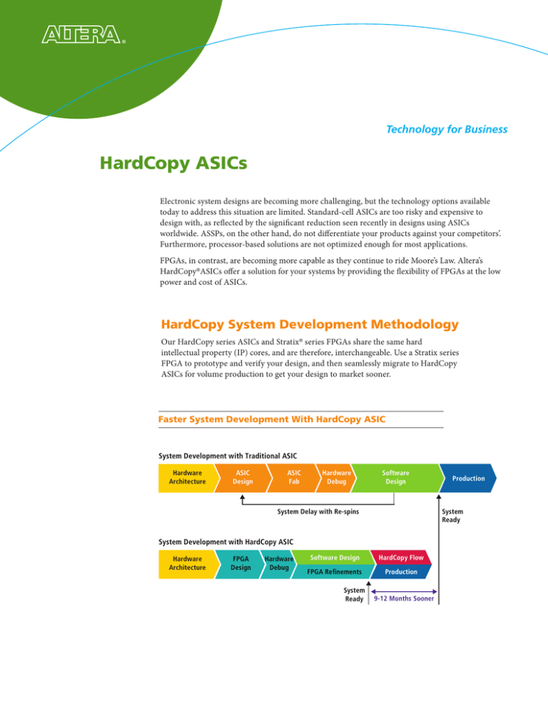
Our HardCopy series ASICs and Stratix® series FPGAs share the same hard
intellectual property (IP) cores, and are therefore, interchangeable. Use a Stratix series
FPGA to prototype and verify your design, and then seamlessly migrate to HardCopy
ASICs for volume production to get your design to market sooner.
Faster System Development With HardCopy ASIC
System Development with Traditional ASIC
Hardware
Architecture
ASIC
Design
ASIC
Fab
Hardware
Debug
Software
Design
System Delay with Re-spins
System
Ready
System Development with HardCopy ASIC
Hardware
Architecture
FPGA
Design
Hardware
Debug
Software Design
HardCopy Flow
FPGA Refinements
Production
System
Ready
Production
9-12 Months Sooner
Design Once for Guaranteed Success
Building upon three generations of HardCopy ASICs, Altera has developed a true “design once” flow for both
HardCopy ASICs and their prototyping FPGAs. At the front end, before design handoff, use one design, one IP set,
one methodology, and one tool to create two device implementations. Get your system ready for production with an
FPGA prototype, and Altera guarantees a functional equivalent and pin-/footprint-compatible HardCopy ASIC as a
drop-in replacement for volume production.
One Design, One RTL, One IP Set, Two Implementations
One RTL
One IP Set
Two Implementations
Design Tool
Fast and Predictable Turnaround Time
When your system is ready, you can perform market testing or initial production with Stratix series FPGAs. If
production requires HardCopy ASICs for power, single event upset (SEU), performance, or cost reasons, Altera’s
HardCopy Design Center provides a fast, predictable, turnkey process that includes full test insertion. You’ll have a
fully tested, production-quality sample in as little as nine weeks, with no design-for-test effort from your own team.
HardCopy Series Design Timeline
Handoff
Tape-out
System Bring-up with FPGA
Prepare Design for Hand-off
Design Center
Implementation
and Verification
Production-quality,
Fully Tested Samples
Custom Mask
Fabrication
Assembly and Test
System
Ready
Sample Approval
Production
~ 3 Weeks
12 Weeks Typical
Time to Samples: 9-14 Weeks
Customers Tell Us
Our customers report that HardCopy ASICs bring:
• Reduced risk – Completely validate systems with the FPGA before switching to the HardCopy device.
• Reduced total cost – Experience low NRE compared with standard-cell ASICs and dramatically reduced total development cost from factors
including a smaller engineering team, faster design and verification time, and inexpensive development tooling cost.
• Faster time to market – Use the FPGA’s flexilibity to speed system verification and software development, and get your system completely
ready for initial production with Stratix series FPGAs prior to ASIC handoff.
• Faster time to profit – Get your system to market sooner and, with the fast and predictable turnaround time to produce a HardCopy ASIC,
quickly turn market share into high-volume profit.
HardCopy IV ASICs
HardCopy IV GX ASICs Product Summary Table
Base Die
HC4GX15
LAF780
HardCopy IV GX
ASIC Packages(1) (2)
HC4GX25
HC4GX25
372, 28, 8+0
LF780
257, 0, 8+0
289, 0, 16+0
LF1152
564, 44, 16+0
FF1152
564, 44, 16+8
564, 44, 16+8
FF1517
744, 88, 24+12
4SGX70
X
4SGX110
X
X
4SGX180
X
X
X
X
X
X
Stratix IV GX FPGA
4SGX230
Prototypes
4SGX290
18 x 18
Max HardCopy IV Multipliers
GX Resources(3)
PLLs
®
Embedded
Memory Bits(5)
X
X
X
X
X
X
X
X
X
X
X
9.2M
9.4M
9.4M
9.4M
11.5M
11.5M
11.5M
1,288
1,040
1,040
1,288
1,288
1,288
1,288
3
3
6
6
6
8
8
8.9 Mb
9.2 Mb
13.3 Mb
13.3 Mb
13.3 Mb
20.3 Mb
20.3 Mb
4SGX530
ASIC Gates
X
X
4SGX360
(4)
X
X
X
X
Notes:
1. LF/LAF: cost-optimized flip chip package; FF: performance-optimized flip chip package.
2. For each device package, the numbers indicates: <Total user I/Os>, <full-duplex LVDS pairs>, <6.5-Gbps physical media attachment (PMA)/physical coding sublayer (PCS) transceiver
channels plus 6.5 Gbps PMA-only channels>. User I/O count includes dedicated input clocks which can be used as data inputs.
3. Device resources shown are the maximum available in the HardCopy base die, the actual usable resource depends on the chosen prototyping FPGA.
4. ASIC gates calculated as 12 gates per logic element (LE) plus 5,000 gates per 18x18 multiplier. Does not include RAMs, phase-locked loops (PLLs), test circuitry and I/O registers.
5. Memory bit count does not include MLAB memories which are constructed with HCells.
HardCopy IV E ASICs Product Summary Table
Base Die
WF484
FF484
HC4E25
HC4E35
296, 48
WF780
392, 48
HardCopy IV E ASIC FF780
Packages(1) (2)
LF1152
FF1152
488, 56
744, 88
LF1517
FF1517
4SE230
Stratix IV E FPGA
Prototypes
880, 88
X
4SE360
X
X
4SE530
X
4SE820
ASIC Gates(4)
18 x 18
Max HardCopy IV E Multipliers
Resources(3)
PLLs
Embedded
Memory Bits(5)
X
X
X
X
9.4M
9.4M
15M
15M
1,288
1,288
1,040
1,040
4
4
8
12
10.7 Mb
12.1 Mb
18.4 Mb
18.4 Mb
Notes:
1. WF: low-cost wire-bond package; LF: cost-optimized flip chip package; FF: performance-optimized flip chip package.
2. For each device package, the numbers indicates: <Total user I/Os>, <full-duplex LVDS pairs>. User I/O count includes dedicated input clocks which can be used as data inputs.
3. Device resources shown are the maximum available in the HardCopy base die, the actual usable resource depends on the chosen prototyping FPGA.
4. ASIC gates calculated as 12 gates per LE plus 5,000 gates per 18x18 multiplier. Does not include RAMs, PLLs, test circuitry and I/O registers.
5. Memory bit count does not include MLAB memories which are constructed with HCells.
Highly Integrated, ASIC-strength Design Tool
Our Quartus® II design software works with our FPGAs and ASICs
to provide a design environment that is easy to use and generates
results quickly. The software provides Synopsys Design Constraint
(SDC)-based synthesis, placement and routing, and static timing
analysis (STA).
Quartus II Software
RTL Synthesis
√
Physical Synthesis
√
Simulation
√
STA (Front End)
√
Detailed Placement
√
Global Routing
√
Incremental Compile
√
Formal Verification
√
Pin Planning
√
Power Estimation
√
More HardCopy ASIC Benefits
HardCopy ASICs also deliver:
• Low power – HardCopy ASICs deliver low levels of power, like that of
standard-cell ASICs. For reduced leakage current, we’ve removed all
unused blocks—RAMs, logic, global clocks, and phase-locked loops
(PLLs)—from the power rail. For low dynamic power, we’ve
implemented hard-wired routing and clocking circuitry in the devices.
HardCopy ASICs can deliver 30 to 70 percent power reduction from the
prototyping FPGAs.
• SEU immunity - HardCopy ASICs are built using an array of
fine-grained HCell blocks that are configured and grouped together by
via programming to construct the FPGA’s combinational and sequential
logic functions and digital signal processing (DSP) blocks. The
connections between HCells are hard-wired after via programming. The
inherent high SEU tolerance of HardCopy ASICs is not only a result of
the hard-wiring, but also due to an improved sequential
elements architecture.
• Higher performance - HardCopy ASICs can provide up to 2X core logic
performance improvement over the FPGA prototype device, due to:
- Removal of programmable switching multiplexers in the FPGA
- Shorter routing from a much smaller die compared with that of
the FPGA
- Fewer logic levels for certain combinatorial logic paths
- Flexibility in HCell macro placement
• Better security – HardCopy ASIC designs are secure from tampering as
there is no device configuration.
• Instant-on – HardCopy ASICs support designs that must power
up instantly.
Want to Dig Deeper?
For more information about designing with HardCopy
ASICs, contact your local Altera sales representative or
FAE, or visit www.altera.com/hardcopy.
Getting Started with HardCopy
ASICs
Systems architected for HardCopy ASICs enable true hardware
and software co-design and tremendously reduce system time to
market and time to profit. The simplicity of using Altera’s
Quartus II design software tool, combined with IP from Altera and
our partners, allows you to design both the FPGA and ASIC
simultaneously. Simply select the appropriate Stratix series FPGA
and HardCopy companion device in the Quartus II software and
start your design—it’s that easy.
Altera Corporation
Altera European Headquarters
Altera Japan Ltd.
Altera International Ltd.
101 Innovation Drive
San Jose, CA 95134
USA
www.altera.com
Holmers Farm Way
High Wycombe
Buckinghamshire
HP12 4XF
United Kingdom
Telephone: (44) 1 94 602 000
Shinjuku i-Land Tower 32F
6-5-1, Nishi-Shinjuku
Shinjuku-ku, Tokyo 163-1332
Japan
Telephone: (81) 3 3340 9480
www.altera.co.jp
Unit 11- 18, 9/F
Millennium City 1, Tower 1
388 Kwun Tong Road
Kwun Tong
Kowloon, Hong Kong
Telephone: (852) 2 945 7000
www.altera.com.cn
Copyright © 2010 Altera Corporation. All rights reserved. Altera, the stylized Altera logo, specific device designations, and all other words and logos that are identified as trademarks and/
or service marks are, unless noted otherwise, the trademarks and service marks of Altera Corporation in the U.S. and other countries. All other product or service names are the property
of their respective holders. Altera products are protected under numerous U.S. and foreign patents and pending applications, mask work rights, and copyrights. PDF; August 2010
SS-01038-2.1
