datasheet

MEMS-G2
MULTIFUNCTION METROLOGY DEVICE WITH UART OUTPUT
FEATURES
Single phase power measurement on a chip.
Compatible with a variety of current sensor technologies.
Simple one-wire UART interface.
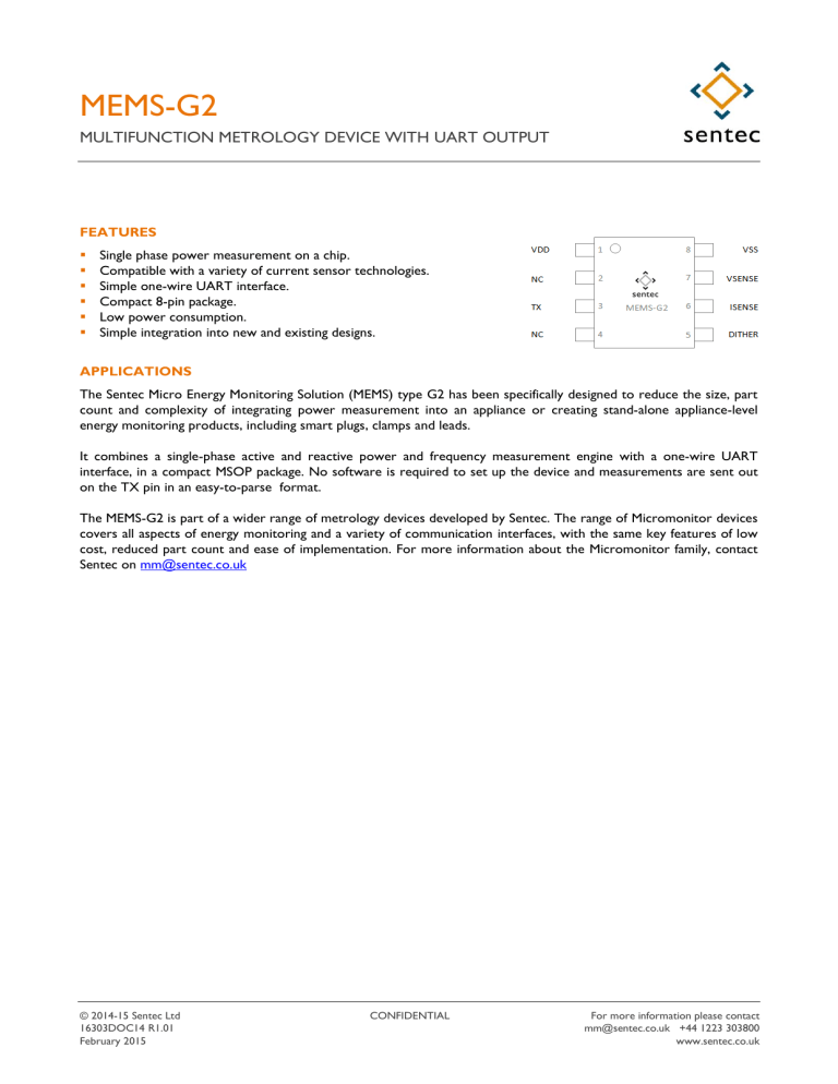
Compact 8-pin package.
Low power consumption.
Simple integration into new and existing designs.
APPLICATIONS
The Sentec Micro Energy Monitoring Solution (MEMS) type G2 has been specifically designed to reduce the size, part count and complexity of integrating power measurement into an appliance or creating stand-alone appliance-level energy monitoring products, including smart plugs, clamps and leads.
It combines a single-phase active and reactive power and frequency measurement engine with a one-wire UART interface, in a compact MSOP package. No software is required to set up the device and measurements are sent out on the TX pin in an easy-to-parse format.
The MEMS-G2 is part of a wider range of metrology devices developed by Sentec. The range of Micromonitor devices covers all aspects of energy monitoring and a variety of communication interfaces, with the same key features of low cost, reduced part count and ease of implementation. For more information about the Micromonitor family, contact
Sentec on mm@sentec.co.uk
© 2014-15 Sentec Ltd
16303DOC14 R1.01
February 2015
CONFIDENTIAL For more information please contact mm@sentec.co.uk +44 1223 303800 www.sentec.co.uk
MEMS-G2 MULTIFUNCTION METROLOGY DEVICE WITH UART OUTPUT
FUNCTIONAL BLOCK DIAGRAM
VDD
ISENSE
VSENSE
DITHER
Current
ADC
Ref
ADC
Voltage
ADC
Acc W
Acc VAR
Acc I²
Acc V²
HPF
HPF
÷
÷
Frequency
π
/
2
× x² x²
× x‾
VAR Cal
V² Cal x‾
I² Cal x‾
W Cal x‾
×
×
×
Acc I²
Acc W
× Acc VAR
Acc V²
√
√
Metrology
Registers
Watts
Vars
RMS
Current
RMS
Voltage
UART
Interface
VSS NC NC
TX
© 2014-15 Sentec Ltd CONFIDENTIAL Page 2 of 9
MEMS-G2 MULTIFUNCTION METROLOGY DEVICE WITH UART OUTPUT
PIN FUNCTION DESCRIPTIONS AND RATINGS
Pin Mnemonic Description
1 VDD Positive supply voltage. 3.3V with respect to V
SS
.
2 NC Not connected.
3
4
TX
NC
UART TX digital output. V
OL
Max = 0.6V, V
OH
Min = V
DD
– 0.7V.
Not connected.
5
6
7
8
DITHER
ISENSE
VSENSE
VSS
DC bias generator with dynamic range enhancement.
Current signal analogue input. The input range is from V
SS to V
SS
+ 2V.
Voltage signal analogue input. The input range is from V
SS to V
SS
+ 2V.
Ground. Reference point for analogue inputs and digital output.
TYPICAL APPLICATION BLOCK DIAGRAM
TYPICAL MEASUREMENT PERFORMANCE
The typical performance of measurements is:
Active power
Reactive power
Voltage
Current
Frequency
±2 W, ±2%; whichever is greater
±2 VAR, ±2%; whichever is greater
±2%
±0.1A, ±2%; whichever is greater
±2%
© 2014-15 Sentec Ltd CONFIDENTIAL Page 3 of 9
MEMS-G2 MULTIFUNCTION METROLOGY DEVICE WITH UART OUTPUT
TYPICAL MEASUREMENT PERFORMANCE
LOW POWER PERFORMANCE
0.0
-2.0
-4.0
-6.0
-8.0
8.0
6.0
4.0
2.0
1 10
Reference Power (W)
100
HIGH POWER PERFORMANCE
8%
6%
4%
2%
0%
-2%
-4%
-6%
-8%
100 1000
Reference Power (W)
These graphs illustrate the typical power measurement performance of the MEMS-G2. At low powers (<100W) the power measurement is within ±2W and at high powers (>100W) the power measurement is within ±2%.
© 2014-15 Sentec Ltd CONFIDENTIAL Page 4 of 9
MEMS-G2 MULTIFUNCTION METROLOGY DEVICE WITH UART OUTPUT
These graphs illustrate the typical reactive power measurement performance of the MEMS-G2. Reactive power
Low Power Performance
8.0
6.0
4.0
2.0
0.0
-2.0
1
-4.0
-6.0
-8.0
10 100
Reference Power (VAR)
High Power Performance
8%
6%
4%
2%
0%
100
-2%
-4%
-6%
-8%
Reference Power (VAR) performance is within ±2VAR or ±2%, whichever the greater.
1000
The graphs were recorded under the following test conditions:
Reference circuit
VDD
Voltage
Power factor
Frequency
Temperature
Implementing example voltage and current input circuits described in this datasheet.
3.3V
230VAC
1.0 for W, 0.1 for VAR
50Hz
25 ° C
© 2014-15 Sentec Ltd CONFIDENTIAL Page 5 of 9
MEMS-G2 MULTIFUNCTION METROLOGY DEVICE WITH UART OUTPUT
SPECIFICATIONS
The Sentec MEMS-G2 is manufactured by Microchip Technology Incorporated.
Footprint*
Packaging
Power consumption
Operating temperature**
MSOP-8
Tape and reel
Typ 1mA @ 3.3V
0 ° C TA +70 ° C
*See www.microchip.com/packaging for package dimensions and recommended land pattern.
**The accuracy of measurements is not guaranteed over the whole temperature range.
ABSOLUTE MAXIMUM RATINGS (†)
Voltage on V
DD
with respect to V
SS
Voltage on all other pins with respect to V
SS
Ambient temperature under bias
Storage temperature
-0.3V to +4.0V
-0.3V to (V
DD
+ 0.3V)
-40°C to +85°C
-65°C to +150°C
† Stresses above those listed under “Absolute Maximum Ratings” may cause permanent damage to the device. This is a stress rating only and functional operation of the device at those or any other conditions above those indicated in the operation listings of this specification is not implied. Exposure above maximum rating conditions for extended periods may affect device reliability.
DESIGN GUIDELINES
The MEMS-G2 is designed to require a minimum number of supporting components. The following notes outline some useful approaches and important considerations when designing for the device. However, Sentec is not liable for customer circuit design, and customers are entirely responsible for their products and applications that incorporate this device.
Off-line power supply
The typical power consumption of the device is 1mA @ 3.3V. This low power consumption allows the use of the device with a low-cost line drop (capacitive or resistive) power supply. The on-chip voltage reference is calibrated from VDD six seconds after power up; it is important that the supply voltage is stable and accurate by this time. The supply voltage must be accurate to 3.3V ± 1% in order to match the accuracy of the chip. Because the voltage reference is used for measurement of current and voltage, a 1% error in VDD will lead to a 2% error in power.
Signal conditioning
The voltage and current signal inputs should be biased to a DC level of V
SS of V
SS
to V
SS
+ 1V and cannot go outside the input range
+ 2V at any time for correct operation of the device. It is recommended that the dither output from the
MEMS-G2 is used to create the bias for the current input as it improves the dynamic range of the measurement – see
Example Current Input Circuit. The device expects analogue inputs proportional to voltage and current. The current channel front end circuitry must contain an integrator for operation with dI/dt Rogowski current sensors.
The input sensitivities are as follows:
Pin
VSENSE
ISENSE
Channel
Voltage
Current
Sensitivity
2.5mV/V
40mV/A
© 2014-15 Sentec Ltd CONFIDENTIAL Page 6 of 9
MEMS-G2 MULTIFUNCTION METROLOGY DEVICE WITH UART OUTPUT
Example Voltage Input Circuit
This design uses R10 and R11 to bias the voltage channel input around ~1V and the resistance ratio of the input chain gives the required voltage channel input signal of 2.5mV/V. The stability and initial accuracy of measurements is dependent on the tolerances of selected components.
Example Current Input Circuit
This design uses a 2mΩ shunt for the current sensor and an op-amp stage with a differential gain of x20 to give the required current channel input signal of 40mV/A. For reference circuits using different current sensors (CT, Rogowski, other values of shunt etc) please contact Sentec.
For both example input circuits the resistor tolerances are ≤1%.
© 2014-15 Sentec Ltd CONFIDENTIAL Page 7 of 9
MEMS-G2 MULTIFUNCTION METROLOGY DEVICE WITH UART OUTPUT
One-wire UART interface
No software or programming is required to set up the device in its default configuration. The following is transmitted out of the TX pin every 5 seconds: p XXXX q XXXX v XX i XX f XXXX
↵ ↓
v i p q f
↵
↓
Real power in W units (16bit signed normal integer) as hexadecimal ASCII
Reactive power in VAR units (16bit signed normal integer) as hexadecimal ASCII
Voltage (rms) in V units (8bit unsigned normal integer) as hexadecimal ASCII
Current (rms) in A units (Unsigned 4.4bit fixed point integer) as hexadecimal ASCII
Frequency in Hz units (Unsigned 8.8bit fixed point integer) as hexadecimal ASCII
Carriage return (CR – value 0x0D)
Line feed (LF – value 0x0A)
Example: p 08FC q 0000 v E6 i A0 f 3200
↵ ↓
p q v i f
One-wire UART settings
Baud
Data bits
Parity
Stop bits
Flow control
38400
8
None
1
None
2300W
0VAR
230V
10.0A
50.0Hz
ORDERING INFORMATION
The Sentec MEMS-G2 may be available for sale by Microchip Technology Incorporated or its affiliates, subject to
Microchip’s terms and conditions of sale.
Sentec part number Microchip catalog number Footprint Packaging Package Marking MOQ
MEMS-G2-eJ
PIC12LF1572T-I/MS023
MSOP-8 Tape and reel Line 1: MSG2eJ 10,000
Line 2: Date code
Smaller quantities for prototyping and early stage manufacturing setup can be obtained directly from Sentec. Contact mm@sentec.co.uk
for more details.
© 2014-15 Sentec Ltd CONFIDENTIAL Page 8 of 9
MEMS-G2 MULTIFUNCTION METROLOGY DEVICE WITH UART OUTPUT
DOCUMENT REVISION
Release
R1.00
R1.01
Comments
Initial release
Production release
TERMS OF USE
Information contained in this publication regarding device applications and the like is provided only for your convenience and may be superseded by updates. It is your responsibility to ensure that your application meets with your specifications. SENTEC LTD MAKES NO REPRESENTATIONS OR WARRANTIES OF ANY KIND WHETHER
EXPRESS OR IMPLIED, WRITTEN OR ORAL, STATUTORY OR OTHERWISE, RELATED TO THE INFORMATION,
INCLUDING BUT NOT LIMITED TO ITS CONDITION, QUALITY, PERFORMANCE, MERCHANTABILITY OR
FITNESS FOR PURPOSE. Sentec Ltd disclaims all liability arising from this information and its use. Use of Sentec Ltd devices in life support and/or safety applications is entirely at the buyer’s risk, and the buyer agrees to defend, indemnify and hold harmless Sentec Ltd from any and all damages, claims, suits, or expenses resulting from such use.
No licenses are conveyed, implicitly or otherwise, under any Sentec Ltd intellectual property rights.
© 2014-15 Sentec Ltd CONFIDENTIAL Page 9 of 9


