4 The TTL Logic Gate Series
advertisement
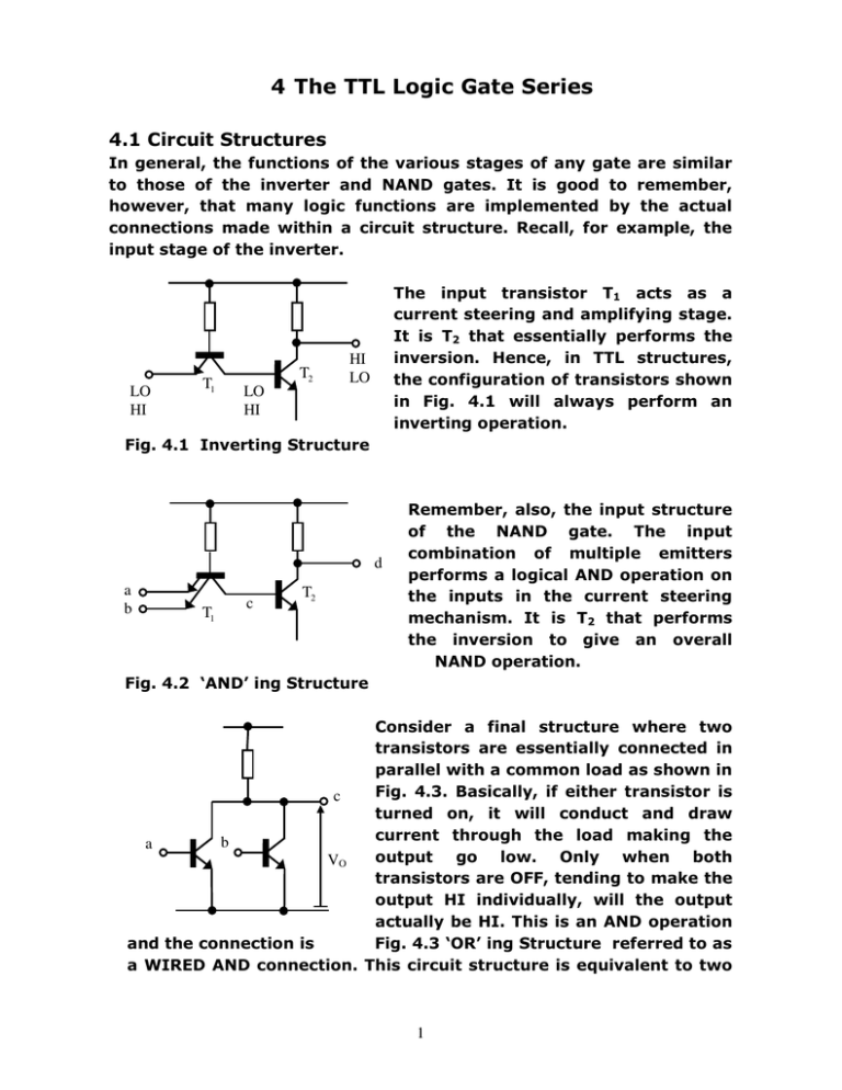
4 The TTL Logic Gate Series 4.1 Circuit Structures In general, the functions of the various stages of any gate are similar to those of the inverter and NAND gates. It is good to remember, however, that many logic functions are implemented by the actual connections made within a circuit structure. Recall, for example, the input stage of the inverter. LO HI T1 T2 The input transistor T1 acts as a current steering and amplifying stage. It is T2 that essentially performs the inversion. Hence, in TTL structures, the configuration of transistors shown in Fig. 4.1 will always perform an inverting operation. HI LO LO HI Fig. 4.1 Inverting Structure d a b T1 c T2 Remember, also, the input structure of the NAND gate. The input combination of multiple emitters performs a logical AND operation on the inputs in the current steering mechanism. It is T2 that performs the inversion to give an overall NAND operation. Fig. 4.2 ‘AND’ ing Structure Consider a final structure where two transistors are essentially connected in parallel with a common load as shown in Fig. 4.3. Basically, if either transistor is c turned on, it will conduct and draw current through the load making the b a output go low. Only when both VO transistors are OFF, tending to make the output HI individually, will the output actually be HI. This is an AND operation and the connection is Fig. 4.3 ‘OR’ ing Structure referred to as a WIRED AND connection. This circuit structure is equivalent to two 1 inverters on the input of an AND gate which is logically equivalent to an NOR structure as can be seen from the table below and Fig. 4.4. ≡ A B C LO LO HI HI LO HI LO HI HI LO LO LO Fig. 4.4 Logical Equivalent of ‘Or’ ing (NOR) Structure 4.2 Standard TTL 74-Series Logic Gates Figs. 4.7 – 4.11 show complete circuit schematic diagrams for some of the basic logic gates in the Standard TTL 7400 series with typical component values included. The diodes shown on the inputs are protection diodes for the input transistors. These prevent negative voltages being developed at input terminals due to ringing on inductive lines used to connect gates together. Large, negative spikes at the input would tend to over bias the base-emitter junction of the input transistors and destroy them. These voltages are clamped to a diode drop by the input protection diodes. (I) Inverter 7404 already covered (II) NAND Gate 7400 (III) NOR Gate 7402 Transistor pairs T1 + T2 and T5 + T6 form inverters to the inputs. The parallel connection of the collectors of T2 and T6 provides a wired AND function as previously described. The output stage, T3 + T4 , is as before. This provides the function a . b = (a + b) which is the NOR operation. (IV) AND-OR-INVERT Gate 7451 This is really a combination of the NAND and NOR gate structures. The multiple emitter input transistors T1 and T5 perform an AND function on their individual inputs. The subsequent transistors T2 and T6 invert the AND functions. The parallel connection of T2 and T6 provides the wired AND function as in the NOR gate. The overall situation is equivalent to that shown in Fig. 4.5. The notable feature of this gate is that it allows Boolean functions to be implemented in sum-of-products 2 form in a single gate with a propagation delay equal to that of an inverter. The inversion of the function can be corrected for by implementing the 0 terms of the function rather than the 1s. a b a b ≡ c d c d a b.c d = a b + c d Fig. 4.5 Logical Equivalent of the AND-OR-INVERT Structure (V) EXCLUSIVE-OR Gate 7486 It can be seen that T1 to T6 of this structure is identical to that of the A-O-I Gate and performs the same logical operation. The transistors T7 + T8 and T9 + T10 simply include an inversion on one pair of inputs. The circuit is logically equivalent to the structure shown in Fig. 4.6 which is seen to provide an exclusive-OR operation. a b a b + a b = a ⊕ b = a ⊕ b → EX − OR Fig. 4.6 Logical Equivalent of the Exclusive OR Gate Structure 3 VCC = 5V INVERTER 7404 R1 R3 130Ω 1.6kΩ RB 4 kΩ T4 D T2 T1 T3 R2 1kΩ Fig. 4.7 Schematic Diagram of the 7404 Standard TTL Inverter VCC = 5V 2-INPUT NAND GATE 7400 R1 RB R3 130Ω 1.6kΩ 4 kΩ T4 D T2 T1 T3 R2 1kΩ Fig. 4.8 Schematic Diagram of the 7400 Standard TTL NAND Gate 4 VCC = 5V 2-INPUT NOR GATE 7402 4 kΩ 1. 6 kΩ 4kΩ 130Ω T4 T2 T1 D T6 T5 T3 1kΩ Fig. 4.9 Schematic Diagram of the 7402 Standard TTL NOR Gate VCC = 5V 4 kΩ 2x2-INPUT AND-OR-INVERT GATE 7451 1.6kΩ 4 kΩ 130Ω T4 T6 T5 D T1 T2 T3 1kΩ Fig. 4.10 Schematic Diagram 7451 Standard TTL AND-OR-INVERT Gate 5 2-INPUT EXCLUSIVE OR GATE 7486 VCC = 5V 4kΩ 4 kΩ 4kΩ 1.6kΩ 4kΩ 130Ω T4 T1 T2 T5 T6 T8 T7 T3 T10 T9 Fig. 4.11 1kΩ Schematic Diagram 7486 Standard TTL EXCLUSIVE-OR Gate 6
