Technology Solutions
Flip Chip Packaging
Demand for flip chip interconnect
technology is being driven by a
number of factors from all corners of
the silicon industry. To support this
demand, Amkor is committed to being
the leading provider of Flip Chip in
Package (FCiP) technology. By
partnering with proven industry
leaders, Amkor has brought high volume packaging and assembly to
the subcontract market. Since being the first OSAT to provide FCiP
solutions in 1999, Amkor has continued to introduce innovative
packaging solutions utilizing Flip Chip interconnect, and offers the
broadest range of FCiP solutions on the market.
Underfill is a specially engineered epoxy that fills the area between the
die and the carrier, surrounding the solder bumps. It is designed to
control the stress in the solder joints caused by the difference in
thermal expansion between the silicon die and the carrier. Once cured,
the underfill absorbs the stress, reducing the strain on the solder
bumps, greatly increasing the life of the finished package. The chip
attach and underfill steps are the basics of flip chip interconnect.
Beyond this, the remainder of package construction surrounding the
die can take many forms and can generally utilize existing
manufacturing processes and package formats.
What is Flip Chip?
Flip Chip (FC) is not a specific package (like SOIC), or even a
package type (like BGA). Flip Chip describes the method of electrically
connecting the die to the package carrier. The package carrier, either
substrate or leadframe, then provides the connection from the die to
the exterior of the package. In "standard" packaging, the
interconnection between the die and the carrier is made using wire.
The die is attached to the carrier face up, then a wire is bonded first to
the die, then looped and bonded to the carrier. Wires are typically
1-5 mm in length, and 15-35 µm in diameter. In contrast, the
interconnection between the die and carrier in flip chip packaging is
made through a conductive "bump" that is placed directly on the die
surface. The bumped die is then "flipped over" and placed face down,
with the bumps­connecting to the carrier directly. A bump is typically
60-100 µm high, and 80-125 µm in diameter.
The flip chip connection is generally formed one of two ways: using
solder or using conductive adhesive. By far, the most common
packaging interconnect is solder. Current solder options are: Eutectic
Sn/Pb or lead-free (98.2% Sn, 1.8% Ag) compositions. The solder
bumped die is attached to a substrate by a solder reflow process, very
similar to the process used to attach BGA balls to the package
exterior. After the die is soldered, underfill is added between the die
and the substrate.
More recent package solution introductions have begun to utilize an
alternative flip-chip interconnect technique called TCNCP (Thermal
Compression Non Conductive Paste). Rather than a two step solderthen-underfill process, TCNCP accomplishes both in a single step.
Solder tipped, non-melting Cu Pillar bumps are pushed through a
liquid epoxy underfill, then heat is applied to both form a metallurgical
bond and cure the epoxy. The use of TCNCP+Cu Pillar allows for finer
bump pitch geometries by maintaining standoff and reducing shorting
issues.
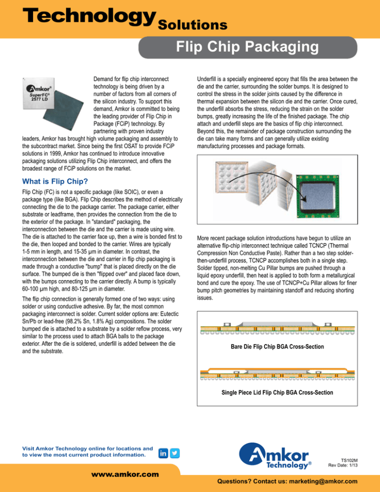
Bare Die Flip Chip BGA Cross-Section
Single Piece Lid Flip Chip BGA Cross-Section
Visit Amkor Technology online for locations and
to view the most current product information.
TS102M
Rev Date: 1/13
Questions? Contact us: marketing@amkor.com
Technology
Solutions
Flip Chip Packaging
Benefits of Flip Chip
Packaging Options Using Flip Chip
Using flip chip interconnect offers a number of possible advantages to
the user:
• Reduced signal inductance – because the interconnect is MUCH
shorter in length (0.1 mm vs. 1-5 mm), the inductance of the signal
path is greatly reduced. This is a key factor in high speed
communication and switching devices
• Reduced power/ground inductance – by using flip chip interconnect,
power can be brought directly into the core of the die, rather than
having to be routed to the edges. This greatly decreases the noise
of the core power, improving performance of the silicon
• Higher signal density – the entire surface of the die can be used for
interconnect, rather than just the edges. This is similar to the
comparison between QFP and BGA packages. Because flip chip
can connect over the surface of the die, it can support vastly larger
numbers of interconnects on the same die size
• Die shrink – for pad limited die (die where size is determined by the
edge space required for bond pads), the size of the die can be
reduced, saving silicon cost
• Reduced package footprint – in some cases, the total package size
can be reduced using flip chip. This can be achieved by either
reducing the die to package edge requirements, since no extra
space is required for wires, or in utilizing higher density substrate
technology, which allows for reduced package pitch
Depending on the specific die and application requirements, different
package level solutions are required. Thus flip chip interconnect can
be used in a wide range of package solutions, each focused on
specific benefits that serve a given market. Amkor offers the widest
possible range of flip chip packaging solutions to meet the diverse
needs of customers and end users. Combining their extensive
manufacturing knowledge with all types of packaging interposers and
further leveraging their leadership role in flip chip interconnect
technology, Amkor continues to pursue new package solutions. This
kind of focus is essential to insure that as new market needs emerge
requiring flip chip interconnect, Amkor is ready with the optimum
package to meet those needs.
Wafer Bumping Technology
In support of Flip Chip assembly,
Amkor has established wafer
bumping production lines within
their Korea, Taiwan and China
manufacturing facilities. Amkor’s
bumping is based on its proprietary
electroplating solder technology
which is considered the most
advanced, robust, reliable and high yielding process available in the
marketplace. Eutectic Sn/Pb, Pb Free (98.2% Sn/1.8% Ag) and Cu
Pillar bumping are all available in volume production on 200 mm and
300 mm wafers.
Features
• Wafer sizes from 150 mm to 300 mm diameter
• Full area array pitch available to 130 µm -- perimeter pad pitch to
<100 µm
• Eutectic Sn/Pb and Pb Free (98.2Sn/1.8Ag) compositions available
• Low alpha (< 0.02 cph) and ultra low alpha (<0.002 cph) solders
available
• Polyimide repassivation available
• Redistribution layer using plated Cu available
Visit Amkor Technology online for locations and
to view the most current product information.
Flip Chip BGA Package
Amkor fcBGA packages are assembled around state-of-the-art, single
unit laminate or ceramic substrates. Utilizing multiple high density
routing layers, laser drilled blind, buried, and stacked vias, and ultra
fine line/space metallization, fcBGA substrates have the highest
routing density available. By combining flip chip interconnect with ultra
advanced substrate technology, fcBGA packages can be electrically
tuned for maximum electrical performance. Once the electrical function
is defined, the design flexibility enabled by flip chip also allows for
significant options in final package design. Amkor offers fcBGA
packaging in a variety of product formats to fit a wide range of end
application requirements.
The variety of fcBGA
package options allows
package selection to be
tailored to the specific
thermal needs of the end
product. High
performance ASIC
products typically utilize a
lidded format that
features a controlled
bondline die attach direct
to a copper heat
spreader. This feature
produces the lowest possible thermal resistance (Theta JC) between
the package and any externally applied thermal solution. The copper
heat spreader effectively spreads heat laterally away from the die to
the package perimeter and into the motherboard.
TS102M
Rev Date: 1/13
Questions? Contact us: marketing@amkor.com
Technology
Solutions
Flip Chip Packaging
Lower wattage products generally utilize bare die or molded
configurations. In these cases, the flip chip construction, with solder
bumps and core vias, provides a lower resistance path from the active
side of the die through the substrate, allowing heat dissipation both
from the package surface and into the motherboard.
This IC packaging technology is applicable for high pin count and/or
high performance ASICs. Large body fcBGAs provide package
solutions for the demands of internet, workstation processors and high
bandwidth system communication devices. By incorporating flip chip
interconnect technology, packages supporting thousands of
connections are enabled in conventional surface mount package
sizes. fcBGAs are also the package of choice for gaming system
processors and graphics, as well as high-end applications processors
for leading-edge portable devices.
FCMBGA (Flip Chip Molded BGA)
FCMBGA is the evolution of the SuperFC® high performance flip chip
solution. Capillary Underfill (CUF) is replaced by Molded Underfill (MUF).
Technology Options
• Substrates
– 4-16 layer laminate build up substrates
– High CTE ceramic
– LTCC Alumina ceramic
– Coreless (in development)
• Bump Types
– Eutectic Sn/Pb
– Pb Free
– Cu Pillar (array and fine pitch peripheral)
• Package Formats
– Bare Die
– Overmolded (FCMBGA)
– Lidded
• 150 µm minimum array bump pitch (130 µm in development)
• <100 µm minimum peripheral bump pitch
• Die sizes up to 26 mm
• Package sizes from 10 mm to 55 mm
• 0.65 mm, 0.8 mm and 1.0 mm pitch BGA footprints
fcBGA/LGA (Bare Die)
Flip chip packaging solution for most graphics, PC chipset and low end ASIC
applications.
Additional Package Options
•
•
•
•
•
•
•
Wafer Node: ≥ 28 nm qualified (20 nm in development)
SMT components on top or bottom side
Multi-die capability
Memory components on top side
Variety of lid material options
Grounded lid
Custom BGA footprints
Visit Amkor Technology online for locations and
to view the most current product information.
fcCeramic CBGA/CLGA/CLLGA/Solder Column Interposer
Original packaging solution for flip chip products.
TS102M
Rev Date: 1/13
Questions? Contact us: marketing@amkor.com
Technology
Solutions
Flip Chip Packaging
fcCSP Package
Flip chip solution for CSP package technology.
Features
•
•
•
•
•
• Designed for high frequency
applications
• Target market – cell phones,
hand-held electronics
• Thin core laminate or ceramic
package construction
Overmolded for handling and second level reliability
Accommodates package sizes from 3 mm to 15 mm
Flip chip bump pitches of 150 µm min. for peripheral array, 250 µm
min. for area array
Available in 0.5-1.0 mm BGA ball pitch, as well as LGA interconnect
Minimum package thickness of 0.80 mm for LGA interconnect,
1.0 mm for 0.5 mm BGA pitch and 1.2 mm for 0.8 mm BGA pitch
Flip Chip SiP Package
Flip Chip SiP package is an extension of the SiP product offering from
Amkor with the device interconnect technology being flip chip rather
than traditional wirebond interconnects. The package may contain
multiple passive components, Silicon and/or GaAs devices bumped
with traditional solder bumps or solder coated 'Copper-Pillar' bumps
housed in 2-Layer or 4-Layer high density substrates. This package
format is gaining traction in RF power amplifier and RF front end
module applications for size, performance and cost reasons.
Controlled collapse of the bumps leads to predictable interconnect
impedance and hence more stable product performance. The low
solder volume in the 'wetting tip' allows for the elimination of the solder
mask from underneath the die which reduces the substrate complexity
and cost and removes a major barrier for adopting the fine pitch FC
interconnection technology in the RF application space. Flip chip
interconnection may also preclude the need for wafer backgrinding (for
mold cap thickness ≥ 0.9 mm) which leads to further reduction in
product cost and simplification of the process flow.
The devices in this application space have low to medium I/O count
and are fairly small in size. This, in conjunction with the solder mask
being removed from underneath the die (which increases the
standoff), makes these products viable candidates for transfer molding
applications. Thus, the underfill operation can be eliminated from the
process flow which leads to significant cost savings. Studies have
shown that transfer molded packages are more reliable (MSL as well
as extended reliability testing such as temperature cycling, HAST, etc.)
than their underfilled counterparts due to balanced die stresses and
better solder CTE matching.
Cu-Pillar or Solder Bump for GaAs and Si Applications in LGA or
BGA Format
Wafer Level Packaging – CSPnl
CSPnl is a true wafer level
package to address improved
second level board reliability,
that incorporates a thin film
redistribution process to route
the pads to JEDEC standard
pitches. Standard "CSP"
solder bumps are formed on
the re-routed pads. The
CSPnl is designed to utilize
standard surface mount
assembly and reflow techniques. By using standard SMT placement
equipment, and avoiding the need for underfill, the end user
experiences many of the cost benefits associated with other JEDEC
standard area array packages.
Features
• Incorporates standard JEDEC pitches and CSP solder ball
diameters
• Compatible with standard SMT assembly and test techniques
• Utilizes cost-effective thin film redistribution technologies
• Backside laser mark compatible
• No need for underfill in most applications
• Full turnkey CSPnl™processing including test and tape and reel
support
• Eutectic lead-free solder balls
• Available with polyimide repassivation
• Qualified and in volume production
• Proven reliability; exceeds all current handset mechanical reliability
tests including: drop, bend and key punch
Visit Amkor Technology online for locations and
to view the most current product information.
With respect to the information in this document, Amkor makes no guarantee or warranty of its accuracy or that the use of such information will not infringe upon the intellectual rights of third parties. Amkor
shall not be responsible for any loss or damage of whatever nature resulting from the use of, or reliance upon it and no patent or other license is implied hereby. This document does not in any way extend
or modify Amkor’s warranty on any product beyond that set forth in its standard terms and conditions of sale. Amkor reserves the right to make changes in its product and specifications at any time and
without notice. © 2013, Amkor Technology Incorporated. All Rights Reserved.
TS102M
Rev Date: 1/13
Questions? Contact us: marketing@amkor.com


