Addressing the Challenges of Small Pad Probing
Technical Brief
InfinityQuad™ Solves Small Pad Probing Challenges
True to the theory of Moore’s Law, leading semiconductor manufacturers’ roadmaps include shrinking devices and
much smaller pads. Numerous advantages come from laying out devices with small pads. Smaller pads not only utilize
less device real estate space, they also allow sacrificial test structures to be placed in scribe lines, meaning process control
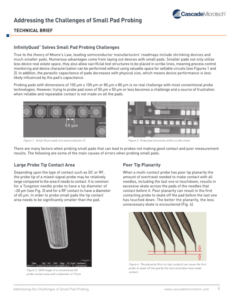
monitoring and device characterization can be performed without using valuable space for sellable circuits (see Figures 1 and
2). In addition, the parasitic capacitance of pads decreases with physical size, which means device performance is less
likely influenced by the pad’s capacitance.
Probing pads with dimensions of 100 µm x 100 µm or 80 µm x 80 µm is no real challenge with most conventional probe
technologies. However, trying to probe pad sizes of 50 µm x 50 µm or less becomes a challenge and a source of frustration
when reliable and repeatable contact is not made on all the pads.
Figure 1. Small 50 µm pads of a semiconductor IC.
Figure 2. Probe pad structures within scribe street.
There are many factors when probing small pads that can lead to probes not making good contact and poor measurement
results. The following are some of the main causes of errors when probing small pads.
Large Probe Tip Contact Area
Poor Tip Planarity
Depending upon the type of contact such as DC or RF,
the probe tip of a mixed-signal probe may be relatively
large compared to the area it needs to contact. It is common
for a Tungsten needle probe to have a tip diameter of
~20 µm (see Fig. 3) and for a RF contact to have a diameter
of 40 µm. In order to probe small pads the tip contact
area needs to be significantly smaller than the pad.
When a multi-contact probe has poor tip planarity the
amount of overtravel needed to make contact with all
needles, including the last one to touchdown, results in
excessive skate across the pads of the needles that
contact before it. Poor planarity can result in the first
contacting probe to skate off the pad before the last one
has touched down. The better the planarity, the less
unnecessary skate is encountered (Fig. 4).
Figure 3. SEM image of a conventional DC
probe contact area with a diameter of 19 µm.
Addressing the Challenges of Small Pad Probing
Figure 4. The planarity (first-to-last contact) can cause the first
probe to skate off the pad by the time all probes have made
contact.
www.cascademicrotech.com
1
Addressing the Challenges of Small Pad Probing
Technical Brief
Overtravel-to-Skate Ratio
Side-Skating Probes
The aforementioned problem is amplified when the
overtravel-to-skate ratio is too small. If a probe has a
1:1 skate ratio then each additional micron of overtravel
needed to bring all tips into contact will result in an
extra micron of skate across the pad (Fig. 5). However,
if a probe has a 4:1 skate ratio then that same micron of
overtravel only results in 0.25 µm of skate.
When a conventional multi-contact probe has many contacts, the needles need to be routed in the shape of a fan
in order to bring all the tips into the tight pitch arrangement of the device under test. This configuration means
that the needles mounted in the center will skate forward
in the direction of the probe, and the probes on the outer
ends enter from an angle and will skate to the side as
well as forward when brought into contact (Fig. 7). This
is known as ‘side skate.’ Side skate limits pad size and
pitch.
Overtravel
Skate
Figure 7. Side-skate causes the outer probe tips to skate inwards, leaving a
wider probe mark and also changing the pitch as extra overtravel is used.
Figure 5. The more over travel applied the more skate occurs. The smaller the
ratio, the more skating effect is suffered by excessive overtravel.
Relative Tip Accuracy
Conventional probes will have mechanical errors in
positioning of each tip relative to each other. These errors
can be in the X, Y and Z axis (Z-axis error is essentially tip
planarity error) and will lead to missing or skating off a
pad, if too extreme (Fig. 6). The better the accuracy of the
tip position, the greater the chance of hitting small pads.
Yaw-Axis Error
Considering the multi-contact probe may have up to
25 contacts and pitches as wide as 250 µm, the overall
length of the probe contact area can be as much as 6 mm.
Unless the probe is aligned perfectly in the yaw-axis
(probe rotation), then the probe tips at the outer ends of
the probe will not be in-line with each other. This needs
to be mechanically corrected by loosening the screws
and manually aligning the yaw-axis by sight, before
tightening the probe mount screws. This method is
problematic and time-consuming, and if not done
correctly the probes will not align with small pads.
Figure 6. A good conventional probe will have up to 10 µm of
tip-to-tip inaccuracy even at ambient temperature.
This probe should have 150 µm even pitch between tips.
High Contact Resistance on Aluminum Pads
Aluminum pads grow a layer of oxide when exposed
to the oxygen in the air. This layer of Aluminum Oxide
needs to be penetrated by the probe in order to make a
low contact resistance measurement. In order to break
through this oxide layer, probes require additional skate
to scrub down to the Aluminum metal below the oxide.
Again, the more scrub the greater the chance of skating
off the pad and losing contact altogether.
Addressing the Challenges of Small Pad Probing
Fig 8. Effect of incorrect yaw alignment
www.cascademicrotech.com
2
Addressing the Challenges of Small Pad Probing
Technical Brief
Net Result of Probe Errors
In effect, each pad has a probing ‘budget.’ Each of the
above errors decreases that budget relative to the size of
the error. For example, if a probe has contact diameter
of 20 µm, a first-to-last of 10 µm (with a 1:1 skate ratio),
has an X & Y accuracy of 10 µm, requires a minimum
skate of 20 µm to break through the oxide and has a side
skate of 45 deg – then the minimum pad size needed to
make repeatable contact with this probe would be 70 µm
long x 65 µm wide, and that is before adding non-probe
related errors of the user, thermal expansion and automatic
probe station accuracies. In this case, a minimum pad size
of 90 µm x 85 µm would be recommended (Fig. 9).
Figure 10. InfinityQuad probe configured with
mixed DC, 20 GHz RF and 110 GHz mm-wave channels.
Because of how the tips are fabricated there is an
extremely small yet durable contact area of 8 µm (long)
x 12 µm (wide) (Fig. 11), very accurate X & Y positional
errors of less than 1 µm (Fig. 12) and first-to-last
planarity of <10 µm (with a 2.5:1 scrub ratio).
Figure11. Small lithographically-fabricated contacts of InfinityQuad with a width of 12 µm and a contacting length of ~ 8 µm.
Figure 9. Footprint of a probing budget when taking into account
errors when using a conventional multi-contact probe.
InfinityQuad Lithographically-Fabricated
Tip Technology
A new multi-contact probe is available from Cascade Microtech
with the introduction of InfinityQuad. InfinityQuad is
the first and only multi-contact probe that uses a
lithographically-fabricated set of tips specifically
designed for probing multiple small pads with mixed
signals. The probe can be configured with up to 25 contacts
that are defined as ground, power (with integrated tip
de-coupling), logic, 20 GHz RF or a premium mmWave
signal up to 110 GHz (Fig. 10).
Addressing the Challenges of Small Pad Probing
Figure 12. Probe marks of InfinityQuad showing X & Y errors of less than 1 µm
at ambient temperature.
The small contact area of the InfinityQuad tip, along with
the hard non-oxidizing Nickel alloy material, provide a
typical contact resistance of less than 50 mΩ with a skate
of less than 16 µm (at 40 µm overtravel). Because the tips are
all skating in parallel to each other, there is zero side skate.
The InfinityQuad enhanced probe mount includes a method to
accurately adjust the yaw-axis to ensure the probe correctly
aligns to the pads. This method is more simple and precise
to set up, saving time and improving probing accuracy.
www.cascademicrotech.com
3
Addressing the Challenges of Small Pad Probing
Technical Brief
Save Probe Pad ‘Budget’
Taking the above into account, the calculated probing
budget is only 14 µm wide and 30 µm long. Including a
conservative allowance for user error, thermal effects and
automatic probing of 10 µm on each side would mean that
the smallest pad InfinityQuad can probe is 30 µm wide and
50 µm long, much smaller than the 90 µm pad budget
with conventional probes (Fig. 13). Manual probing,
probing at ambient temperature only or using advanced
unattended over-temperature probe station software such
as VueTrack™ from Cascade Microtech, could potentially
allow a pad budget as small as ~20 µm x 30 µm.
Measurements Over Full Thermal Range
The thermal repeatability of InfinityQuad is superior to
other conventional probe technologies, however, tolerances
of probe tip accuracy at different temperatures does have
an effect. The magnitude of the effect depends on the
number of contacts and the pitch (which determines the
physical width of the whole probe) and the thermal range.
When probing over the full specified range of InfinityQuad
from -40ºC to +125ºC, the minimum recommended pad
sizes for the number of tips and pitch are shown in Table 1.
It should be noted that these recommendations take into
account all the error margins of measuring over the full
thermal range when used in an automatic mode on
a Cascade Microtech semi-automatic probe station.
Results may vary with other manual, semi-automatic and
fully automatic probe stations.
Figure 13. Footprint of the InfinityQuad probing budget uses 1/10 of the
surface area compared to a conventional probe.
Table 1. Recommended minimum pad sizes dependent upon number of contacts and pitch. Numbers are inclusive of probing budget and an error window representative of user error, auto-prober error and thermal effects.
Addressing the Challenges of Small Pad Probing
www.cascademicrotech.com
4
Addressing the Challenges of Small Pad Probing
Technical Brief
Conclusion
InfinityQuad technology reduces the minimum size of the
pad that can be used with a multi-contact, mixed-signal
probe (Fig. 14). Pads as small as 30 µm x 50 µm become
a reality in automated over-temperature probing applications.
This allows the user to reduce pad sizes, saves device
real estate space (Fig. 15) and lowers pad parasitics – both
saving money and improving measurement accuracy. And
for customers already using small pads, InfinityQuad
will allow confidence in making contact with the pad
repeatedly – reducing the amount of time needed to
manually test or eliminating the need to repeat automatic
tests due to probes skating off the pads.
Example of minimum pad
footprint of a conventional
multi-contact probe
Minimum
InfinityQuad
pad footprint
Figure 14. A good example of a conventional probe mark compared to an
InfinityQuad probe mark using a similar scale.
Figure 15. Including an error margin for automatic probing over temperature,
the recommended pad area for InfinityQuad is five times less than
conventional probes.
InfinityQuad is the only multi-contact probe technology
that allows automatic measurements of small pads over
temperature.
© Copyright 2012 Cascade Microtech, Inc.
All rights reserved. Cascade Microtech is
a registered trademark, and InfinityQuad
is a trademark of Cascade Microtech, Inc.
All other trademarks are the property
of their respective owners.
Cascade Microtech, Inc.
Corporate Headquarters
toll free: +1-800-550-3279
phone: +1-503-601-1000
email: cmi_sales@cmicro.com
Data subject to change without notice.
Germany
phone: +49-89-9090195-0
email: cmg_sales@cmicro.com
Singapore
phone: +65-6873-7482
email: cms_sales@cmicro.com
Japan
phone: +81-3-5615-5150
email: cmj_sales@cmicro.com
Taiwan
phone: +886-3-5722810
email: cmt_sales@cmicro.com
China
phone: +86-21-3330-3188
email: cmc_sales@cmicro.com
SmallPadProbing_InfQuad_0212
Addressing the Challenges of Small Pad Probing
www.cascademicrotech.com
5


