Design and Optimization of Lumped Element Hybrid Couplers
advertisement
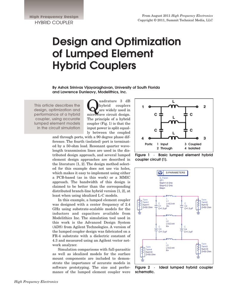
From August 2011 High Frequency Electronics Copyright © 2011, Summit Technical Media, LLC High Frequency Design HYBRID COUPLER Design and Optimization of Lumped Element Hybrid Couplers By Ashok Srinivas Vijayaraghavan, University of South Florida and Lawrence Dunleavy, Modelithics, Inc. Q uadrature 3 dB hybrid couplers are widely used in microwave circuit design. The principle of a hybrid coupler (Fig. 1) is that the input power is split equally between the coupled and through ports, with a 90 degree phase difference. The fourth (isolated) port is terminated by a 50-ohm load. Resonant quarter wavelength transmission lines are used in the distributed design approach, and several lumped element design approaches are described in the literature [1, 2]. The design method selected for this example does not use via holes, which makes it easy to implement using either a PCB-based (as in this work) or a MMIC approach. The bandwidth of this design is claimed to be better than the corresponding distributed branch-line hybrid version [1, 2], at least when using idealized L-C models. In this example, a lumped element coupler was designed with a center frequency of 2.4 GHz using substrate-scalable models for the inductors and capacitors available from Modelithics Inc. The simulation tool used in this work is the Advanced Design System (ADS) from Agilent Technologies. A version of the lumped coupler design was fabricated on a FR-4 substrate with a dielectric constant of 4.3 and measured using an Agilent vector network analyzer. Simulation comparisons with full-parasitic as well as idealized models for the surface mount components are included to demonstrate the importance of accurate models in software prototyping. The size and performance of the lumped element coupler were This article describes the design, optimization and performance of a hybrid coupler, using accurate lumped element models in the circuit simulation High Frequency Electronics Ports: 1 Input 2 Through 3 Coupled 4 Isolated Figure 1 · Basic lumped element hybrid coupler circuit [1]. Figure 2 · schematic. Ideal lumped hybrid coupler High Frequency Design HYBRID COUPLER compared to a distributed branchline 3 dB coupler designed at the same frequency. A lumped hybrid coupler such as this may be used in I-Q modulators and demodulators, in balanced amplifiers for VSWR improvement at the input and to increase output power at the output, in single-ended mixer design, and other circuits. Ideal Design and Simulation The initial step in the proposed design methodology is to synthesize the nominal values of inductors and capacitors based on the design frequency followed by simulating the ideal design using the ideal lumped element models (Fig. 2). The following equations were used to synthesize the element values based on the frequency and characteristic impedance [1, 2]. Figure 3 · S parameter response of ideal lumped element coupler. Figure 4 · Phase response of ideal lumped element coupler. L = Z0 / (2π f) nH C = 1 / (Z0 2π f) pF The S parameter response and the phase response of the ideal lumped element coupler is as shown in Figures 3 and 4 for: Port Port Port Port 1—Input port 2—Through port 3—Coupled port 4—Isolated Port The second step was to replace the ideal models with Modelithics parasitic models and observe the shift in the parameters of interest (S11, S21, S31, S41 in Figures 5 and 6). Transmission line effects were added to the previous schematic, using built-in ADS “MLIN,” “MTEE” and “MSTEP” microstrip elements. Figure 7 shows the new schematic; Figure 8 is the constructed coupler. The updated response is as shown in Figures 9 and 10. The response was optimized with a goal of matching the S parameter performance of the ideal design. The L-C part values and the dimensions of the transmission lines High Frequency Electronics Figure 5 · S parameter response of coupler with Modelithics models. Lumped Before After Elements Optimization Optimization (Ideal) (Real) L1 3.3 nH 1.5 nH L2 3.3 nH 1.5 nH L3 3.3 nH 1.5 nH C1 1.3 pF 3 pF C2 1.3 pF 3 pF C3 1.3 pF 3 pF C4 1.3 pF 3 pF Table 1 · Inductor and capacitor values before and after optimization. were allowed to vary, without changing the symmetry of the coupler, and constraining the part values to available ranges. Table 1 shows component values, before and after optimization. Table 2 shows the widths and lengths of the transmission lines in the layout, Figure 6 · Phase response of coupler with Modelithics models. Dimension Before After Optimization Optimization Wa (mm) 5 5.6 La (mm) 20 7.11 Wb (mm) 5 2.2 Lb (mm) 20 19.9 Table 2 · Dimension of the widths and lengths (MLIN, MSTEP, MTEE) before and after optimization. (Wb, Lb = width, length along vertical; Wa, La = width, length along horizontal). which are optimized without changing the symmetry of the layout, where: • Wa — Width of the TL along the horizontal of the layout • La — Length of the TL along the horizontal of the layout High Frequency Design HYBRID COUPLER Figure 8 · Layout of the hybrid coupler (top) using ADS and a photo of the constructed unit (bottom). • Wb — Width of the TL along the vertical of the layout • Lb — Length of the TL along the vertical of the layout Layout of the Lumped Coupler The layout of the lumped coupler was generated using ADS and was used for electromagnetic analysis using Momentum. The simulated electromagnetic results were very close to the circuit simulations using discontinuities. Distributed Coupler at 2.4 GHz Figure 7 · Schematic of the lumped coupler with transmission line effects. High Frequency Electronics A branch-line distributed coupler was designed at 2.4 GHz for comparison purposes. The length and width of the transmission lines were calculated using Linecalc for the ideal design. All the discontinuities like MTEE’s MSTEP’s were included. The simulated response was narrow band when compared to the lumped element response. The response of this High Frequency Design HYBRID COUPLER (a) (a) (a) (b) (b) (b) Figure 9 · Measured to modeled results for coupling (a) at port 2 and (b) port 3. Black line is measured; red line is modeled. Figure 10 · Measured to modeled results for (a) Return loss and (b) Isolation. Black line is measured; red line is modeled. distributed version is compared to all the lumped element version ables to which tolerance could be added in the circuit. After reviewing manufacturer data sheet information, the following tolerances were used: 10% for inductors, 5% for capacitors, 5% for substrate thickness and 5% t for the dielectric constant. The statistical value type form used was Uniform during simulation. Monte Carlo Tolerance Analysis A Monte Carlo tolerance analysis was done to analyze the sensitivity of the lumped element coupler to the thickness of the substrate, dielectric constant and the part value tolerance. The Monte Carlo analysis simulation was run for 30 simulation trials using ADS. The analysis used all the four yield specifications for S11, S21, S31 and S41. The data for all the 30 trials were saved and plotted. The expression here refers to return loss to be at least –25 dB. I used three more similar yield specifications for isolation, and insertion loss at coupling ports. Inductor (a), capacitor (b), substrate thickness (Hs), and dielectric constant (Ef) were the variHigh Frequency Electronics Figure 12 · Performance comparison of lumped coupler with the distributed version at 2.4 GHz (a) S11 (b) Isolation. Blue line is distributed; red line is lumped. Conclusion Based on the design literature [1] a hybrid lumped element coupler was designed at 2.4 GHz. Passive accurate models (Modelithics) were used during simulation. The measured to modeled results of the coupler are presented. A Monte Carlo analysis was performed taking into account the board and lumped element tolerances, and the results are presented. Acknowledgement The authors would like to thank Mr. Luis Ledezma, graduate student at University of South Florida, for helping with electromagnetic simulations. References Figure 11 · S parameter response of an ideal distributed coupler. 1. Jian-An Hou and Yeong-Her Wang, “A compact quadrature hybrid based on high-pass and low-pass lumped elements,” IEEE Microw. Wireless Compon. Lett., vol. 17, no. 8, pp. 595-597, Aug. 2007. 2. Yi-Chyun Chiang and Chong-Yi Figure 13 · Performance (S parameters) comparison of lumped coupler with the distributed version at 2.4 GHz; (a) coupling at port 2 (b) coupling at port 3. Blue line is distributed; red line is lumped. Figure 14 · Tolerance analysis of: (a) return loss and (b) coupling at port 2 (simulated) of the lumped coupler. Black line is measured; red line is modeled. Chen, “Design of a wide band lumped element 3 db quadrature coupler,” IEEE Transactions on Microwave theory and Techniques, vol. 49, no.3, pp. 476-479, March 2001. 3. Jion-An Hou and Yeong-her Wang, “Design and analysis of novel quadrature hybrids with compact lumped elements,” International Symposium on Microwave and Optical Technology, pp. 536-539, Dec. 2009. 4. David M.Pozar, Microwave Engineering, 3rd edition, John Wiley and Sons, pp. 308-361. 5. David Andrews, Lumped Element Quadrature Hybrid, Artech House, 2006. Figure 15 · Tolerance analysis of: (a) coupling at port 3 and (b) isolation (simulated) of the lumped coupler. Black line is measured; red line is modeled. Author Information Ashok Srinivas Vijayaraghavan is a graduate student in the Wireless and Microwave Information Systems (WAMI) group, Department of Electrical Engineering, University of South Florida. He can be reached by e-mail at: ashoksriniva@mail.usf.edu Dr. Larry Dunleavy is one of the founders and President of Modelithics, Inc. He received his BSEE from Michigan Tech, and the MSEE and PhD degrees from the University of Michigan. He was one of the faculty group that founded the WAMI Center at USF, where he maintains an appointment as a part time professor. He can be reached at: ldunleavy@modelithics.com August 2011
