Lab 5: BJT Amplifiers – Part II
advertisement

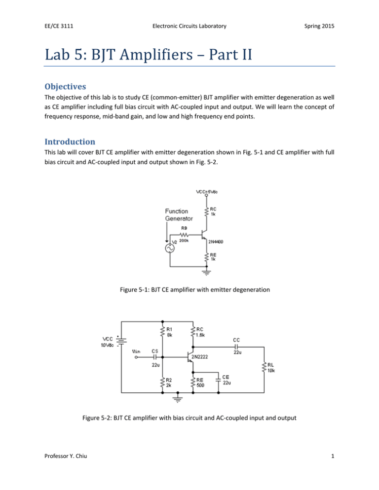
EE/CE 3111 Electronic Circuits Laboratory Spring 2015 Lab5:BJTAmplifiers–PartII Objectives The objective of this lab is to study CE (common‐emitter) BJT amplifier with emitter degeneration as well as CE amplifier including full bias circuit with AC‐coupled input and output. We will learn the concept of frequency response, mid‐band gain, and low and high frequency end points. Introduction This lab will cover BJT CE amplifier with emitter degeneration shown in Fig. 5‐1 and CE amplifier with full bias circuit and AC‐coupled input and output shown in Fig. 5‐2. Figure 5‐1: BJT CE amplifier with emitter degeneration Figure 5‐2: BJT CE amplifier with bias circuit and AC‐coupled input and output Professor Y. Chiu 1 EE/CE 3111 Electronic Circuits Laboratory Spring 2015 DC Analysis To ensure that the circuit functions as an amplifier, we need to first make sure that the BJT is biased properly in the FAR. In Fig. 5‐1, this is accomplished by choosing the right DC voltage of the input. Note that the collector of the BJT (i.e., amplifier output) should measure a voltage close to VCC/2 when everything works properly. To analyze the operating point of the BJT, we can overlay the I‐V characteristic of the BJT‐RE combo – IC vs. the absolute value of VC, not VCE as in Lab 4 – with the load line. It is important that you treat the BJT and RE as a composite device here, i.e., the emitter of the composite BJT now is the other terminal of RE. In Fig. 5‐2, the circuit biasing is accomplished with the resistors R1, R2, and RE. Again, we can plot the I‐V characteristic of the BJT‐RE combo and the load line to identify the operating point of the BJT. To obtain maximum output swing, the transistor should be biased in the middle of the linear gain region, i.e., the Q (quiescent) bias point. To determine the BJT current at the Q point in Fig. 5‐2, we can write the following equations for the emitter and base currents VCC IE R2 Vf R2 R1 , I B I E RE F 1 (5‐1) where Vf is the turn‐on voltage of the base‐emitter junction and βF is the DC current gain (IC/IB) of the BJT. Note that (βF + 1)RE >> R1 || R2 is assumed in order to arrive at the IE expression in Eq. (5‐1). Figure 5‐3: AC equivalent circuit of the amplifier in Fig. 5‐2 AC Analysis AC analysis refers to the small‐signal linear analysis of the amplifier equivalent circuit shown in Fig. 5‐3, where RB = R1 || R2. Note that here the BJT symbol has been replaced by the so‐called “hybrid‐π” equivalent circuit model. We are interested in finding out the frequency response and the mid‐band gain of the amplifier. Frequency response of the circuit derives from the capacitive elements in the circuit. For example, CS, CC, and CE are AC‐coupling capacitors, i.e., for frequencies reasonably higher than DC, they can be considered as short circuits, while Cπ and Cμ are inherent capacitance of the BJT that will lead to high‐frequency roll‐offs for the amplifier gain. Combining the two effects at low and high frequencies, the gain exhibits a low cutoff frequency and a high cutoff frequency as well as a middle part that is flat or frequency independent. The flat gain of the middle part is referred to as the mid‐band Professor Y. Chiu 2 EE/CE 3111 Electronic Circuits Laboratory Spring 2015 gain, and the low and high cutoff frequencies are simply the frequency points at which the mid‐band gain decreases by 3 dB. Since the mid‐band gain is independent of frequency, we can short all AC‐coupling capacitors (CS, CC, and CE) and open all high‐frequency capacitors (Cπ and Cμ) in the equivalent circuit and obtain the following mid‐band equivalent circuit Figure 5‐4: Mid‐band AC equivalent circuit of the amplifier in Fig. 5‐2 and the mid‐band gain can be determined as Amid g m RC / / RL (5‐2) Preparation 1. Simulate in PSpice the CE amplifier in Fig. 5‐1. Obtain the transfer function of the amplifier. Determine the DC input voltage to bias the BJT in the center of the linear region. Compare this result with your hand calculation. Determine the small‐signal (AC) gain of the amplifier at the operating point above and compare with your hand calculation. 2. Simulate in PSpice the frequency response of the amplifier in Fig. 5‐2. Perform a DC operating point analysis and find out the emitter and base currents and compare with your hand calculation. You may assume βF = 100 and Vf = 0.7V in your hand calculation. You may then apply an AC voltage source as Vin and determine the ratio Vout/Vin as a function of frequency. Mark the mid‐band gain and the low and high cutoff frequency points. Compare the gain with your hand calculation. Procedure 1. CE amplifier with emitter degeneration (Fig. 5‐1) Measure the I‐V characteristic of the BJT‐RE composite transistor using BJT_IV_curve.vi (Note: plot the collector current as a function of the absolute collector voltage instead of VCE). Draw the load line of the amplifier in Fig. 5‐1 on top of the I‐V curves. Use the program tranchar.vi to measure the transfer function of the amplifier. Use the information from the above steps to find the DC voltage of the input needed to place Professor Y. Chiu 3 EE/CE 3111 Electronic Circuits Laboratory Spring 2015 the BJT operating point in the middle of the linear region of the transfer function. Use the function generator as the input source, and set it up as follows o Waveform: sinusoidal o Offset: the DC input voltage you found o Amplitude: 0.1V o Frequency: 1kHz Use the oscilloscope to view the input and output waveforms. Record the small‐signal (AC) voltage gain and the DC values of the collector voltage and the collector current. Increase the amplitude of the function generator until you see the output clipped at the top and bottom of the sine wave. Then use the XY display mode of the oscilloscope, and set the input signal to Channel 1 and the output signal to Channel 2. What you will see here is the transfer function of the amplifier. Use the cursors to measure the maximum and minimum output voltages. 2. CE amplifier with bias circuit and AC‐coupled input and output (Fig. 5‐2) Measure the I‐V characteristic of the BJT‐RE composite transistor using BJT_IV_curve.vi. Draw the load line of the amplifier in Fig. 5‐2 on top of the I‐V curves. Determine the collector current and the Q point. Use the collector current you found to determine the gm of the BJT and compute the mid‐band gain of the amplifier using Eq. (5‐2). Build the circuit in Fig. 5‐2. Since the voltage gain of this amplifier is large (>100), we can modify the circuit in the following two ways (one at a time not both) to lower its gain. a. Replace RL by a small resistor of around 100 Ohm. b. Remove the emitter degeneration bypass capacitor CE. Set the input signal to sine wave at 100 kHz with an amplitude of 0.1V, and measure the mid‐ band gain of the amplifier using either a) or b) from the last step. If the gain is still a bit large, tune down the amplitude of your sine‐wave generator to avoid saturating your amplifier. Use freqlog.vi to obtain the Bode plot for the gain. Record the mid‐band gain and mark the high and low frequency end points for the mid‐band region. Analysis 1. With the modifications of RL or CE in the second amplifier, the Bode plot you measured in the lab will differ from that you simulated for the prelab. Perform the simulations again with these modifications. Do your simulation results agree with measurements now? 2. It is easy to understand why RL influences the amplifier gain while it is not that straightforward to understand the CE effect. Could you argue why removing CE impact the gain so greatly? Calculate the gain by hand and compare to your measurement and simulation results. Professor Y. Chiu 4 EE/CE 3111 Electronic Circuits Laboratory Spring 2015 Lab 5 Report Instructions Besides the general guidelines, report the following for this lab: CE amplifier with emitter degeneration 1. Plot I-V curves for BJT + RE combo with load line, show load line equation used. 2. Sketch (by hand, PSpice or any drawing program) the circuit. 3. Plot Vout vs. Vin curve (transfer function), show the range of the linear gain region (Vin,min, Vout,max) and (Vout,min, Vout,max) and AC gain computed from the slope. 4. Show Vin,middle and Vout,middle in linear region. 5. Show AC gain obtained from oscilloscope readings, and the DC values of the Vout and Iout. 6. Show the Vin value to achieve Vout clipping. Explain why clipping occurred at this value. CE amplifier with bias circuit and AC-coupled input and output 1. Plot I-V curves for BJT + RE combo with load line, show load line equation used. Mark the Q point. 2. Sketch (by hand, PSpice or any drawing program) the circuit. 3. Show the Bode plots you measured for the amplifier and clearly mark the high and low frequency end points and the mid-band gain. Report this for the RL and CE modifications separately. Answer the questions in the Analysis section. Professor Y. Chiu 5

