CMD225 - Custom MMIC
advertisement
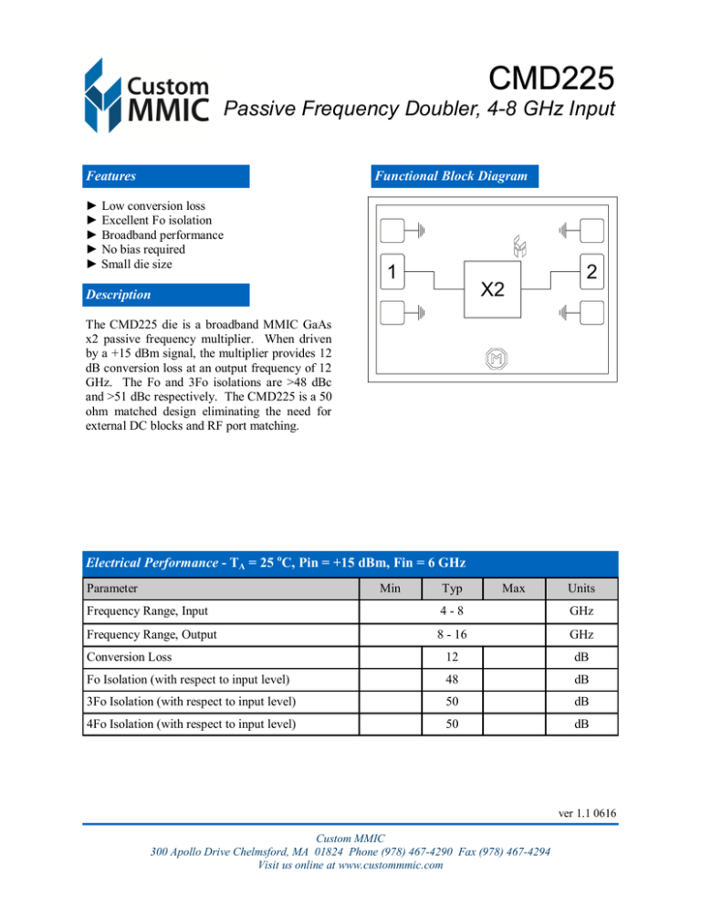
CMD225 Passive Frequency Doubler, 4-8 GHz Input Features Functional Block Diagram ► Low conversion loss ► Excellent Fo isolation ► Broadband performance ► No bias required ► Small die size 1 2 X2 Description The CMD225 die is a broadband MMIC GaAs x2 passive frequency multiplier. When driven by a +15 dBm signal, the multiplier provides 12 dB conversion loss at an output frequency of 12 GHz. The Fo and 3Fo isolations are >48 dBc and >51 dBc respectively. The CMD225 is a 50 ohm matched design eliminating the need for external DC blocks and RF port matching. Electrical Performance - TA = 25 oC, Pin = +15 dBm, Fin = 6 GHz Parameter Min Typ Max Units Frequency Range, Input 4-8 GHz Frequency Range, Output 8 - 16 GHz Conversion Loss 12 dB Fo Isolation (with respect to input level) 48 dB 3Fo Isolation (with respect to input level) 50 dB 4Fo Isolation (with respect to input level) 50 dB ver 1.1 0616 Custom MMIC 300 Apollo Drive Chelmsford, MA 01824 Phone (978) 467-4290 Fax (978) 467-4294 Visit us online at www.custommmic.com CMD225 Passive Frequency Doubler, 4-8 GHz Input Specifications Absolute Maximum Ratings Parameter Rating RF Input Power +27 dBm Operating Temperature -55 to 85 °C Storage Temperature -55 to 150 °C Operation of this device outside the maximum ratings may cause permanent damage. Electrical Specifications - TA = 25 oC, Pin = +15 dBm Parameter Min Typ Max Min Typ Max Units Frequency Range, Input 4-8 5-7 GHz Frequency Range, Output 8 - 16 10 - 14 GHz Conversion Loss 12 19 12 16 dB Fo Isolation (with respect to input level) 33 48 38 48 dB 3Fo Isolation (with respect to input level) 43 50 43 50 dB 4Fo Isolation (with respect to input level) 23 50 33 50 dB ver 1.1 0616 Custom MMIC 300 Apollo Drive Chelmsford, MA 01824 Phone (978) 467-4290 Fax (978) 467-4294 Visit us online at www.custommmic.com CMD225 Passive Frequency Doubler, 4-8 GHz Input Typical Performance Conversion Gain vs. Temperature @ +15 dBm Drive Level 0 +25C +85C -5 -55C Conversion Gain/dB -10 -15 -20 -25 -30 -35 -40 4 4.5 5 5.5 6 6.5 7 7.5 8 7 7.5 8 Input Frequency/GHz Conversion Gain vs. Drive Level, TA = 25 oC 0 -5 Conversion Gain/dB -10 -15 -20 +9 dBm +11 dBm +13 dBm +15 dBm +17 dBm +19 dBm -25 -30 -35 -40 4 4.5 5 5.5 6 6.5 Input Frequency/GHz Custom MMIC 300 Apollo Drive Chelmsford, MA 01824 Phone (978) 467-4290 Fax (978) 467-4294 Visit us online at www.custommmic.com ver 1.1 0616 CMD225 Passive Frequency Doubler, 4-8 GHz Input Typical Performance Isolation (with respect to input level) @ +15 dBm Drive Level, TA = 25 oC 0 Fo -10 3Fo 4Fo -20 Isolation/dB -30 -40 -50 -60 -70 -80 -90 -100 0 2 4 6 8 10 12 14 16 18 20 22 24 26 28 30 32 Frequency/GHz Input Return Loss @ +15 dBm Drive Level, TA = 25 oC 0 Return Loss/dB -5 -10 -15 -20 -25 4 4.5 5 5.5 6 6.5 7 7.5 8 Input Frequency/GHz Custom MMIC 300 Apollo Drive Chelmsford, MA 01824 Phone (978) 467-4290 Fax (978) 467-4294 Visit us online at www.custommmic.com ver 1.1 0616 CMD225 Passive Frequency Doubler, 4-8 GHz Input Typical Performance Output Return Loss @ +15 dBm Drive Level, F = 6 GHz Input, TA = 25 oC 0 Return Loss/dB -5 -10 -15 -20 -25 8 9 10 11 12 13 14 15 16 Output Frequency/GHz ver 1.1 0616 Custom MMIC 300 Apollo Drive Chelmsford, MA 01824 Phone (978) 467-4290 Fax (978) 467-4294 Visit us online at www.custommmic.com CMD225 Passive Frequency Doubler, 4-8 GHz Input Mechanical Information Die Outline (all dimensions in microns) 1 2 790.00 470.00 104.00 1060.00 Notes: 1. No connection required for unlabeled pads 2. Backside is RF and DC ground 3. Backside and bond pad metal: Gold 4. Die is 100 microns thick 5. DC bond pads are 100 microns square ver 1.1 0616 Custom MMIC 300 Apollo Drive Chelmsford, MA 01824 Phone (978) 467-4290 Fax (978) 467-4294 Visit us online at www.custommmic.com CMD225 Passive Frequency Doubler, 4-8 GHz Input Pin Description Pad Diagram 1 2 Functional Description Pad Function Description Schematic RF in 1 RF in Pad is DC coupled and 50 ohm matched RF out 2 RF out Pad is DC coupled and 50 ohm matched Backside Ground Connect to RF / DC ground GND ver 1.1 0616 Custom MMIC 300 Apollo Drive Chelmsford, MA 01824 Phone (978) 467-4290 Fax (978) 467-4294 Visit us online at www.custommmic.com CMD225 Passive Frequency Doubler, 4-8 GHz Input Applications Information Assembly Guidelines The backside of the CMD225 is RF ground. Die attach should be accomplished with electrically and thermally conductive epoxy or eutectic attach. Standard assembly procedures should be followed for high frequency devices. The top surface of the semiconductor should be made planar to the adjacent RF transmission lines. RF connections should be made as short as possible to reduce the inductive effect of the bond wire. Use of a 0.8 mil thermosonic wedge bonding is highly recommended as the loop height will be minimized. The RF input and output require a single bond wire as shown. The semiconductor is 100 um thick and should be handled by the sides of the die or with a custom collet. Do not make contact directly with the die surface as this will damage the monolithic circuitry. Handle with care. Assembly Diagram RF in RF out GaAs MMIC devices are susceptible to damage from Electrostatic Discharge. Proper precautions should be observed during handling, assembly and test. ver 1.1 0616 Custom MMIC 300 Apollo Drive Chelmsford, MA 01824 Phone (978) 467-4290 Fax (978) 467-4294 Visit us online at www.custommmic.com


