MOSFET current voltage characteristics
advertisement
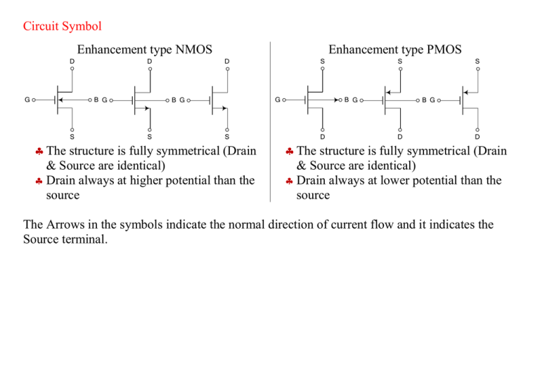
Circuit Symbol Enhancement type NMOS D G D B G S Enhancement type PMOS D G B G S S S The structure is fully symmetrical (Drain & Source are identical) Drain always at higher potential than the source S B G D S B G D D The structure is fully symmetrical (Drain & Source are identical) Drain always at lower potential than the source The Arrows in the symbols indicate the normal direction of current flow and it indicates the Source terminal. Current-voltage characteristics: iD-vDS D iD S vGS iG iS = iD vDS vDS iG vGS S iS = iD D iD (mA) iD iD (mA) VDS VGS Vt Triode Region VSD VGS Vt VDS VGS Vt Saturation Region VGS Vt (cut off ) Triode Region VSD VGS Vt Saturation Region VGS=Vt+5 VGS=Vt - 5 VGS=Vt+4 VGS=Vt - 4 VGS=Vt+3 VGS=Vt - 3 VGS=Vt+2 VGS=Vt - 2 VGS=Vt+1 VGS=Vt - 1 VDS (V) VGS Vt (cut off ) VSD (V) Three distinct regions of operation: 1. Cut-off Region 2. Triode Region 3. Saturation Region Saturation region: used for amplifier applications Cut-off & Triode Region: used for Switch applications PMOS NMOS Voltage S Triode Vt |Vt| Overdrive voltage D Overdrive voltage Threshold Threshold G |Vt| D Saturation Vt Saturation G S Triode Voltage Relative terminal voltage of the enhancement type NMOS and PMOS for operation in the # regions NMOS PMOS I - vGS ≤ Vt No channel cut-off Region 𝑖𝐷 = 0 I - vGS ≥ Vt No channel cut-off Region 𝑖𝐷 = 0 II - vGS > Vt Induced channel II - vGS < Vt Induced channel 1) vDS ≤ vGS - Vt; ( vGD ≥ Vt ) 1) vDS ≥ vGS - Vt; (continuous channel) Triode Region 𝑖𝐷 = 𝑘𝑛′ (continuous channel) Triode Region 𝑊 1 2 𝑣𝐺𝑆 − 𝑉𝑡 ∙ 𝑣𝐷𝑆 − 𝑣𝐷𝑆 𝐿 2 𝑘𝑛′ ≡ Process Transconductance Parameter 𝑊 ≡ Aspect Ratio 𝐿 For vDS very small, Linear relation ⇒ Operation like resistor rDS 𝑖𝐷 = 𝑘𝑝′ 𝑊 1 2 𝑣𝐺𝑆 − 𝑉𝑡 ∙ 𝑣𝐷𝑆 − 𝑣𝐷𝑆 𝐿 2 𝑘𝑝′ ≡ Process Transconductance Parameter 𝑊 𝐿 ≡ Aspect Ratio For |vDS| very small, Linear relation ⇒ Operation like resistor rDS 2) vDS ≥ vGS - Vt; ( vGD ≤ Vt ) (pinched-off channel) Saturation Region 1 𝑊 𝑖𝐷 = 𝑘𝑛′ 𝑣 − 𝑉𝑡 2 𝐿 𝐺𝑆 ( vGD ≤ Vt ) 2 2) vDS ≤ vGS - Vt; ( vGD ≥ Vt ) (pinched-off channel) Saturation Region 1 ′ 𝑊 𝑖 𝐷 = 𝑘𝑛 𝑣 − 𝑉𝑡 2 𝐿 𝐺𝑆 2 Role of the Substrate Body Effect In many application Source and Body are connected ⇒ Substrate does not have any role All the above characterization is valid with no change In Integrated Circuit (IC) the body is common to many MOS transistors: In NMOS the body is connected to the lowest voltage In PMOS the body is connected to the highest voltage The resulting reverse bias between Source and Body VSB will have an effect on the operation: This effect can be simply represented by a change in the threshold voltage: 𝑉𝑡 = 𝑉𝑡0 + 𝛾 2𝜙𝑓 + 𝑉𝑆𝐵 − 2𝜙𝑓 𝑉𝑡0 ≡ Threshold at VSB = 0; 𝜙𝑓 ≡ Physical parameter; typically 2𝜙𝑓 ~ 0.6 𝑉 𝛾= 2𝑞𝑁𝐴 𝜀 𝑠 𝐶𝑜𝑥 ≡ is a fabrication process parameter; typically 𝛾 ~ 0.4 V1/2

