Ultra Low Noise Amplifiers
advertisement
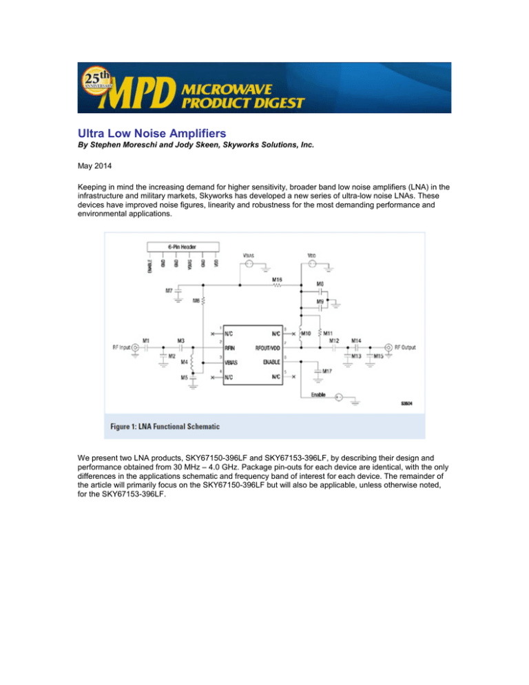
Ultra Low Noise Amplifiers By Stephen Moreschi and Jody Skeen, Skyworks Solutions, Inc. May 2014 Keeping in mind the increasing demand for higher sensitivity, broader band low noise amplifiers (LNA) in the infrastructure and military markets, Skyworks has developed a new series of ultra-low noise LNAs. These devices have improved noise figures, linearity and robustness for the most demanding performance and environmental applications. We present two LNA products, SKY67150-396LF and SKY67153-396LF, by describing their design and performance obtained from 30 MHz – 4.0 GHz. Package pin-outs for each device are identical, with the only differences in the applications schematic and frequency band of interest for each device. The remainder of the article will primarily focus on the SKY67150-396LF but will also be applicable, unless otherwise noted, for the SKY67153-396LF. The primary function of the LNA is to minimize the cascaded noise figure (NF) of the receiver. As described by the Friis equation, the LNA gain minimizes the cascaded NF impact of subsequent stages and its low NF minimizes its own NF contribution. This resulting low cascaded NF results in optimal receiver sensitivity in low signal level conditions and thus, the LNA is a common receiver element in the vast majority of receiver architectures. In addition to its gain and NF characteristics, the LNA linearity should also be high enough so that this stage does not limit the cascaded input third order intercept point ((IIP3) and input 1 dB compression point (IP1dB) of the receiver. The family of products presented here are ultra-high performance, low noise single stage amplifiers designed for wireless applications in the 30 MHz to 4.0 GHz band of interest. Targeted applications are any systems requiring ultra low noise figures, very good linearity and extended temperature performance to +105ºC ambient. These single stage high linearity, high gain low noise GaAs pHEMT amplifiers are housed in a low thermal resistance 8-pin 2X2 mm2 package. Thermal performance is also improved by the use of a low resistance high conductivity thermal epoxy which is used to attach the GaAs amplifier die to the package lead frame. This attachment method as well as rugged on-die structures gives the devices the ability to operate safely up to the +105ºC maximum ambient temperature. The LNA's active bias circuitry internally provides stable performance over temperature and process variations. Supply current is also controlled by adjusting one external resistor and can be varied over a very wide range independently from the device Vdd. This feature allows the device efficiency to be optimized according to the linearity requirements of a particular application. Any additional technical information required can be made available by Skyworks. If a new application from a customer requires a specialized tuning, requests may be forwarded as well. Design and Configuration Figure 1 shows the active biasing and matching circuits required for the device to operate properly. The operating current will be set through the external resistor component, M6. A typical set of bias current vs. resistor values is shown in Figure 2. The recommended range of bias current for operating the modules is from 25mA–110mA, with operating voltages that can range from 3.0V– 5.0V. Operating the devices anywhere within these ranges of bias conditions will result in excellent performance. Generally speaking, higher device quiescent current will result in higher IIP3, while higher Vdd will result in higher IP1dB. Gain (S(2,1)) and NF are relatively insensitive to device Iddq and measured results indicate little performance advantage from device currents higher than 100 mA. Referring to Figure 1, components M1, M2, M3, and M4 are used for matching Input Return Loss (S(1,1)) as well as NF. M4 also acts as a high impedance bias supply for the gate of the input FET, with M5 acting as an RF short circuit at the frequency of operation. For optimal NF, all the input matching components should have high Q with wire-wound inductors, offering an excellent combination of price and performance. Component M10 acts as a high impedance bias feed for the drain of the output FET as well as part of the matching for output return loss (S(2,2)). Capacitor M9 is also part of the bias structure and acts as a short circuit to ground at the RF frequency of interest. It can also be used to match S(2,2) as well, but to a lesser degree than Inductor M10. Resistor M11, which is in parallel with M10, tends to de-Q the output match and this small resistive loading tends to provide extra stability margin, especially at high frequency. A very minor degradation in gain, IP3 and P1dB is incurred, but the effect is quite minimal at less than 0.5dB. Components M12, M13, M14 and M15 are all for output matching and are used mostly for the tuning of S(2,2), IP3 and P1dB. High frequency stability is again also improved with the addition of resistor M15 with very minor degradations in performance as noted above. All devices on the output side of the amplifier can be standard Q components with no significant performance impact. Both the SKY67150-396LF and the SKY67153-396LF have an enable or power down feature which is present on pin 7. The enable feature is active on a low signal input, <0.20V and in this condition the amplifier is in the “ON” state. Levels above 1.50 V up to a maximum of 5.5V will turn the amplifier to the “OFF” state and current consumption will be approximately 1.5 mA. Note that when in the “OFF” conditions, RF signal levels of 0dBm or more will begin to re-bias the gate of the input transistor and the device will begin to turn back on to some degree. For applications in which the device must remain off under high input power levels, it is recommended that the Vdd be switched low to prevent this self-biasing from occurring. Figure 3 shows the evaluation board (EVB) used to test and tune the LNA in its different tuning states. The board is comprised of a four-layer stack with the top layer being Rogers 4350B, 0.254 mm or 10 mils thick. Transmission line construction is coplanar with a ground plane spacing of 0.394 mm and via diameters are all 0.254 mm. Careful attention to the layout must be employed to reduce the risk of stray capacitance or inductance, which may result in decreased performance or instabilities in the device at especially high frequencies. Ground vias under the device must also be as detailed in Figure 4. An insufficient amount of ground via or those with increased inductance will increase the thermal resistance of the device, lowering its maximum operating temperature, as well as potentially inducing high frequency instabilities in the amplifier from increased source inductance. Typical Performance Data There are a variety of matching structures which can be employed to cover as an example the performance of the SKY67150-396LF from 30 MHz to 2200 MHz. For this example, consider the tuning from 650MHz to 1100 MHz. Figures 5-9 highlight the typical small signal performance at 5V and 82mA. The device has been tuned for lowest NF in this example, while still maintaining a reasonable S(1,1) of -11.3dB. The measured noise figure of the complete evaluation board with this particular set of matching components was found to be 0.25dB at 849MHz. This extremely low noise figure actually challenges the accuracy of the measurement equipment, which has on its own uncertainty factor for the measurement. The device can also be tuned if required for best S(1,1) at the expense of slightly degraded noise figure. As an example, with an S(1,1) of approx. -18dB or less, the measured NF would degrade to 0.30 to 0.35dB. Gain (S(2,1)) for the device under these conditions was 20.5dB and S(2,2) was measured to be -20dB. Note also that the even with this excellent output match and high gain the output IP3 was +39dBm or equivalently +18.5dBm input IP3 Output compression point was also measured to be +21dBm (OP1dB), +15.dBm(IP1dB). So, not only is the SKY67150-396LF an ultra-low noise amplifier which was primarily designed as an input or stage-one amplifier, it also has the ability to be a stage-two device because of its excellent linearity characteristics. The device also yields very good reverse isolation (S12), +28.0dBm, making it very insensitive to load matching while trying to match the input for lowest noise or best S11. Stability vs. frequency and temperature is shown in Figures 10 and 11. Stability factors vs. bias voltage and current stay quite uniform and controlled. It is important that the applications circuit grounding of the device paddle be adhered to (Figure 4). This will ensure a good thermal contact as well as provide a low inductance path to ground for terminating RF currents. Low Frequency Performance Data By revising the application circuit slightly, the SKY67150-396LF also has the ability to extend down to 30MHz. Resistive feedback from output of the device directly back to the input of the device has been added, as shown in Figure 12. This feedback results in a low NF solution with excellent linearity and stability, along with good input and output return losses. Typical low frequency performance at 100MHz with this feedback present is shown in Table 1. This is a clear example of the outstanding performance capability of this LNA over a wide range of application frequencies. SKY67150-396LF Frequency Response Data Shown in Table 1 is the frequency banded performance of the SKY67150-396LF. Please note however that the lowest frequency tuning, 30MHz- 400MHz, requires the addition of an extra feedback path,which is shown in Figure 12. Table 2 highlights the frequency banded performance of the SKY67153-396LF. Two new ultra low noise LNAs in 2 x 2 mm2 8-pin packages have been presented. Both devices achieve extremely low noise figure, excellent stability, high linearity and gain using simple external matching circuits which allow these devices to cover a frequency range of 30 MHz to 3.8 GHz and beyond. Their excellent linearity characteristics allow these devices to be used as both first and second stage LNAs and they can provide outstanding solutions for linear driver transmit applications as well. The various device application schematics offer solutions over the full application frequency range with unconditional stability over the full operating temperature range of -40ºC to +105ºC. Further, we have shown that these devices can also be operated over a wide range of current and voltages, thus allowing optimal efficiency given the linearity requirements of a particular application. Their outstanding performance at low voltages and currents makes these devices ideal for high efficiency, high performance battery powered applications. Finally, the thermal characteristics of these parts allow them to achieve high long term reliability and excellent performance up to an ambient temperature of +105ºC, making the devices ideal for applications with demanding environmental conditions such as military, automotive and cellular infrastructure. For additional information on each of these devices, please refer to the data sheets which are located at our website. Skyworks Solutions, Inc. www.skyworksinc.com
