Questions 1 Question 4.1–1: (Solution, p 4) Draw two truth tables
advertisement

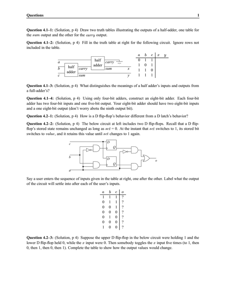
Questions 1 Question 4.1–1: (Solution, p 4) Draw two truth tables illustrating the outputs of a half-adder, one table for the output and the other for the output. Question 4.1–2: (Solution, p 4) Fill in the truth table at right for the following circuit. Ignore rows not included in the table. a b c half carry adder sum half carry adder sum x y 0 1 1 1 1 0 1 1 1 1 0 1 Question 4.1–3: (Solution, p 4) What distinguishes the meanings of a half adder’s inputs and outputs from a full-adder’s? Question 4.1–4: (Solution, p 4) Using only four-bit adders, construct an eight-bit adder. Each four-bit adder has two four-bit inputs and one five-bit output. Your eight-bit adder should have two eight-bit inputs and a one eight-bit output (don’t worry abotu the ninth output bit). Question 4.2–1: (Solution, p 4) How is a D flip-flop’s behavior different from a D latch’s behavior? Question 4.2–2: (Solution, p 4) The below circuit at left includes two D flip-flops. Recall that a D flipflop’s stored state remains unchanged as long as = 0. At the instant that switches to 1, its stored bit switches to , and it retains this value until changes to 1 again. D c Q b D o Q a Say a user enters the sequence of inputs given in the table at right, one after the other. Label what the output of the circuit will settle into after each of the user’s inputs. 1 0 0 0 0 0 1 1 1 0 0 1 0 0 1 1 1 0 0 0 0 ? ? ? ? ? ? ? Question 4.2–3: (Solution, p 4) Suppose the upper D flip-flop in the below circuit were holding 1 and the lower D flip-flop held 0, while the input were 0. Then somebody toggles the input five times (to 1, then 0, then 1, then 0, then 1). Complete the table to show how the output values would change. Questions 2 D Q1 Q x D Q Q0 0 1 0 1 0 1 1 0 Question 5.1–1: (Solution, p 5) Define the fetch-execute cycle as it relates to a computer processing a program. Your definition should describe the primary purpose of each phase. Question 5.1–2: (Solution, p 5) Explain in detail what HYMN does during the fetch phase of the fetchexecute cycle. Question 5.1–3: (Solution, p 5) Translate each of the following HYMN instructions into machine code. Express your answers in binary. a. HALT 12 03 b. ADD 14 c. LOAD d. JUMP Question 5.1–4: (Solution, p 5) Suppose our computer starts with the following in memory. addr 00000 00001 00010 00011 00100 00101 data 100 00100 110 00101 111 00100 101 00111 000 00101 000 00110 translation LOAD 00100 ADD 00101 SUB 00100 STORE 00111 HALT HALT a. Show the hexadecimal values taken on by the registers as this program executes. (Stop once the computer executes a HALT instruction.) IR PC AC b. What memory locations, if any, change? What values are stored in these locations? Question 5.2–1: (Solution, p 5) Suppose we were to start the computer with the following in memory. addr 00000 00001 00010 00011 00100 00101 00111 data 100 11110 101 11111 110 11110 101 11111 110 11110 101 11111 000 00000 translation LOAD 11110 STORE 11111 ADD 11110 STORE 11111 ADD 11110 STORE 11111 HALT Questions 3 If the user typed multiples of 25 starting at 25 (25, then 50, then 75,. . . ) when prompted, what would the computer display? Question 5.2–2: (Solution, p 5) Suppose we were to start the computer with the following in memory. addr 00000 00001 00010 00011 If we repeatedly type the number 32 computer halts? data 100 11110 110 11110 010 00001 000 00000 translation LOAD 11110 ADD 11110 JPOS 00001 HALT when prompted, how many times would we type it before the Question 5.2–3: (Solution, p 5) What should we place into the computer’s memory so that, when started, to 64 before halting? the computer displays the powers of two from 1 Solutions 4 Solution 4.1–1: (Question, p 1) 0 0 1 1 Solution 4.1–2: (Question, p 1) 0 1 1 1 0 1 0 1 0 1 1 0 1 0 1 1 1 1 0 1 0 0 1 1 0 1 0 1 0 0 0 1 1 1 1 0 0 1 1 0 Solution 4.1–3: (Question, p 1) A half adder has two inputs and outputs the sum of these two bits, while a full adder has three inputs and outputs the sum of these three bits. b4-7 4-bit adder a4-7 4-bit adder b0-3 4-bit adder Solution 4.1–4: (Question, p 1) The design of this circuit is similar in structure to the design of a full adder using half adders. a0-3 out0-3 out4-7 0 Solution 4.2–1: (Question, p 1) In a D flip-flop, the memory value changes only at that instant that the input becomes 1. In a latch, however, the memory value continues adopting any values given as long as its input is 1. (In a D flip-flop, if the input changes while remains 1, the remembered value doesn’t change. In a latch, however, the input changing while is 1 results in a change to the remembered value.) Solution 4.2–2: (Question, p 1) Solution 4.2–3: (Question, p 1) 0 1 0 1 0 1 1 0 0 0 0 1 0 0 0 1 1 0 1 0 0 0 0 0 1 1 1 0 0 1 0 0 1 1 1 0 0 0 0 1 1 1 1 0 0 1 Solutions 5 Solution 5.1–1: (Question, p 2) The fetch-execute cycle is the process by which a classical computer executes instructions. In the fetch phase, the computer determines the next instruction to be completed by fetching the instruction from memory. In the execute phase, the computer executes this instruction. Solution 5.1–2: (Question, p 2) It loads from memory from the address contained in the PC, storing the data found there into the IR. Solution 5.1–3: (Question, p 2) a. 000 00000 b. 110 10100 c. 100 10010 d. 001 00011 Solution 5.1–4: (Question, p 2) a. IR PC AC 84 C5 E4 A5 00 00 01 02 03 04 05 0B 06 b. Memory location 00111 changes to hold 06 . Solution 5.2–1: (Question, p 2) ? 25 25 ? 50 75 ? 75 -106 , but (This last output is somewhat tricky: In the last ADD instruction, the CPU computes this exceeds the maximum eight-bit two’s-complement number. So the computer wraps around ends up at .) Solution 5.2–2: (Question, p 3) It would read from the user four times before halting (with the AC pro gressing from to to to ). Solution 5.2–3: (Question, p 3) Here is one possible solution. (Of course there are others.) addr 00000 00001 00010 00011 00100 00101 00110 data 100 00110 101 11111 101 00111 110 00111 010 00001 000 00000 000 00001 translation LOAD 00110 STOR 11111 STOR 00111 ADD 00111 JPOS 00001 HALT 1


