QUAD 2-INPUT SCHMITT TRIGGER NAND GATE SN54/74LS132
advertisement
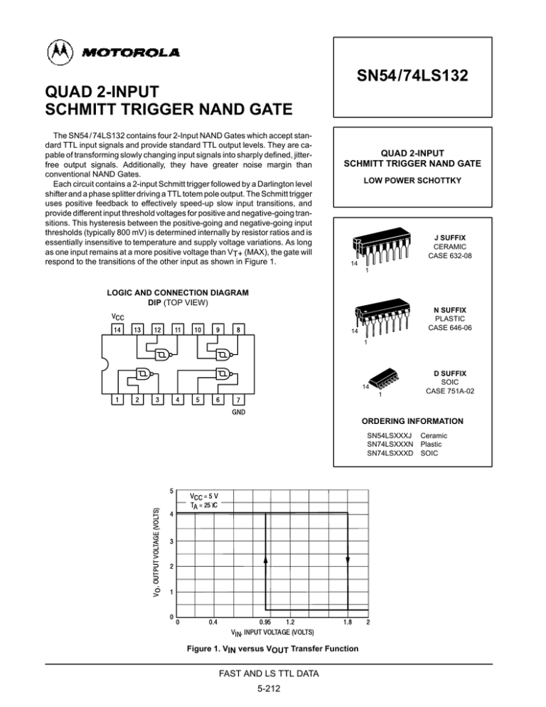
SN54/74LS132 QUAD 2-INPUT SCHMITT TRIGGER NAND GATE The SN54 / 74LS132 contains four 2-Input NAND Gates which accept standard TTL input signals and provide standard TTL output levels. They are capable of transforming slowly changing input signals into sharply defined, jitterfree output signals. Additionally, they have greater noise margin than conventional NAND Gates. Each circuit contains a 2-input Schmitt trigger followed by a Darlington level shifter and a phase splitter driving a TTL totem pole output. The Schmitt trigger uses positive feedback to effectively speed-up slow input transitions, and provide different input threshold voltages for positive and negative-going transitions. This hysteresis between the positive-going and negative-going input thresholds (typically 800 mV) is determined internally by resistor ratios and is essentially insensitive to temperature and supply voltage variations. As long as one input remains at a more positive voltage than VT+ (MAX), the gate will respond to the transitions of the other input as shown in Figure 1. QUAD 2-INPUT SCHMITT TRIGGER NAND GATE LOW POWER SCHOTTKY J SUFFIX CERAMIC CASE 632-08 14 1 LOGIC AND CONNECTION DIAGRAM DIP (TOP VIEW) N SUFFIX PLASTIC CASE 646-06 14 1 14 1 ORDERING INFORMATION SN54LSXXXJ SN74LSXXXN SN74LSXXXD D SUFFIX SOIC CASE 751A-02 ° Figure 1. VIN versus VOUT Transfer Function FAST AND LS TTL DATA 5-212 Ceramic Plastic SOIC SN54/74LS132 GUARANTEED OPERATING RANGES Symbol Parameter Min Typ Max Unit VCC Supply Voltage 54 74 4.5 4.75 5.0 5.0 5.5 5.25 V TA Operating Ambient Temperature Range 54 74 – 55 0 25 25 125 70 °C IOH Output Current — High 54, 74 – 0.4 mA IOL Output Current — Low 54 74 4.0 8.0 mA DC CHARACTERISTICS OVER OPERATING TEMPERATURE RANGE (unless otherwise specified) Limits Symbol Min Parameter Typ Max Unit Test Conditions VT+ Positive-Going Threshold Voltage 1.5 2.0 V VCC = 5.0 V VT– Negative-Going Threshold Voltage 0.6 1.1 V VCC = 5.0 V VT + – VT– Hysteresis 0.4 V VCC = 5.0 V VIK Input Clamp Diode Voltage V VCC = MIN, IIN = – 18 mA V VCC = MIN, IOH = – 400 µA, VIN = VIL 0.8 – 0.65 54 2.5 3.4 74 2.7 3.4 – 1.5 VOH Output HIGH Voltage VOL Output LOW Voltage IT+ Input Current at Positive-Going Threshold – 0.14 mA VCC = 5.0 V, VIN = VT+ IT– Input Current at Negative-Going Threshold – 0.18 mA VCC = 5.0 V, VIN = VT– IIH Input HIGH Current IIL Input LOW Current IOS Output Short Circuit Current (Note 1) ICC 54, 74 0.25 0.4 V VCC = MIN, IOL = 4.0 mA, VIN = 2.0 V 74 0.35 0.5 V VCC = MIN, IOL = 8.0 mA, VIN = 2.0 V – 20 20 µA VCC = MAX, VIN = 2.7 V 0.1 mA VCC = MAX, VIN = 7.0 V – 0.4 mA VCC = MAX, VIN = 0.4 V –100 mA VCC = MAX, VOUT = 0 V Power Supply Current Total, Output HIGH 5.9 11 mA VCC = MAX, VIN = 0 V Total, Output LOW 8.2 14 mA VCC = MAX, VIN = 4.5 V Max Unit Test Conditions VCC = 5.0 V CL = 15 pF Note 1: Not more than one output should be shorted at a time, nor for more than 1 second. AC CHARACTERISTICS (TA = 25°C) Limits Symbol Parameter Min Typ tPLH Turn-Off Delay, Input to Output 22 ns tPHL Turn-On Delay, Input to Output 22 ns Figure 2. AC Waveforms FAST AND LS TTL DATA 5-213 SN54/74LS132 ° !!$"! ∆ $ "&!" $ " $ " ∆ $" $ " " !$"$"! " $ % !#& $" $"! Figure 3. Threshold Voltage and Hysteresis versus Power Supply Voltage $ !!$"! ∆ $ "&!" " " !$"$"! $ " $ " ° ° ∆ $" ° ° " " " "# ° Figure 4. Threshold Voltage and Hysteresis versus Temperature FAST AND LS TTL DATA 5-214 ° Case 751A-02 D Suffix 14-Pin Plastic SO-14 "! !! ( ( ! " " ! " # %# (" ! "# !# -A- 8 P -B1 ! #! " #! ! * ! !" $ !" M J F R X 45° K D " ! ! " * C G " 7 & 14 "#! ! ! ! ° ° ° ° ) ) ) ) Case 632-08 J Suffix 14-Pin Ceramic Dual In-Line -A- "! ! " ! & 14 8 " ! " " -B1 ! 7 * " -T- L G J " ! & # * !" $ !" " M N D ! " * K F $ " $ " " C $ & ! ! ! ! ° ! ° ° ° ) ) ) ) Case 646-06 N Suffix 14-Pin Plastic "! 14 " B 1 A ! ( ! " # # F L C J N K M FAST AND LS TTL DATA 5-215 ! " * !" $ !" D ! $ ! H #! " " ! ( " " 7 G ! $" '' !" " !" " %# 8 * ! ! ! ° ° ! ° ° # Motorola reserves the right to make changes without further notice to any products herein. Motorola makes no warranty, representation or guarantee regarding the suitability of its products for any particular purpose, nor does Motorola assume any liability arising out of the application or use of any product or circuit, and specifically disclaims any and all liability, including without limitation consequential or incidental damages. “Typical” parameters can and do vary in different applications. All operating parameters, including “Typicals” must be validated for each customer application by customer’s technical experts. Motorola does not convey any license under its patent rights nor the rights of others. Motorola products are not designed, intended, or authorized for use as components in systems intended for surgical implant into the body, or other applications intended to support or sustain life, or for any other application in which the failure of the Motorola product could create a situation where personal injury or death may occur. Should Buyer purchase or use Motorola products for any such unintended or unauthorized application, Buyer shall indemnify and hold Motorola and its officers, employees, subsidiaries, affiliates, and distributors harmless against all claims, costs, damages, and expenses, and reasonable attorney fees arising out of, directly or indirectly, any claim of personal injury or death associated with such unintended or unauthorized use, even if such claim alleges that Motorola was negligent regarding the design or manufacture of the part. Motorola and are registered trademarks of Motorola, Inc. Motorola, Inc. is an Equal Opportunity/Affirmative Action Employer. Literature Distribution Centers: USA: Motorola Literature Distribution; P.O. Box 20912; Phoenix, Arizona 85036. EUROPE: Motorola Ltd.; European Literature Centre; 88 Tanners Drive, Blakelands, Milton Keynes, MK14 5BP, England. JAPAN: Nippon Motorola Ltd.; 4-32-1, Nishi-Gotanda, Shinagawa-ku, Tokyo 141, Japan. ASIA PACIFIC: Motorola Semiconductors H.K. Ltd.; Silicon Harbour Center, No. 2 Dai King Street, Tai Po Industrial Estate, Tai Po, N.T., Hong Kong. ◊ FAST AND LS TTL DATA 5-216


