AC Analysis of a Common-Emitter Amplifier
advertisement

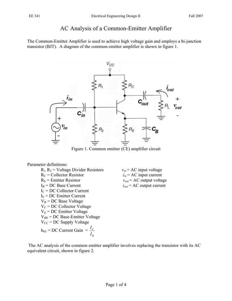
EE 341 Electrical Engineering Design II Fall 2007 AC Analysis of a Common-Emitter Amplifier The Common-Emitter Amplifier is used to achieve high voltage gain and employs a bi-junction transistor (BJT). A diagram of the common-emitter amplifier is shown in figure 1. Figure 1. Common emitter (CE) amplifier circuit Parameter definitions: R1, R2 = Voltage Divider Resistors RC = Collector Resistor RE = Emitter Resistor IB = DC Base Current IC = DC Collector Current IE = DC Emitter Current VB = DC Base Voltage VC = DC Collector Voltage VE = DC Emitter Voltage VBE = DC Base-Emitter Voltage VCC = DC Supply Voltage I hFE = DC Current Gain = C IB vin = AC input voltage iin = AC input current vout = AC output voltage iout = AC output current The AC analysis of the common emitter amplifier involves replacing the transistor with its AC equivalent circuit, shown in figure 2. Page 1 of 4 EE 341 Electrical Engineering Design II Fall 2007 Figure 2. AC equivalent circuit of a bi-junction transistor The parameters of this equivalent circuit are: ib = AC base current ic = AC collector current ie = AC emitter current ic ib rbe = Internal AC resistance of the base-emitter junction hfe = AC Current Gain = The value of the AC current gain (hfe) is typically fairly close to the DC current gain (hFE). The AC resistance of the base-emitter junction (rbe) is calculated from: rbe = 0.025 where IE = DC Emitter Current IE Since this is a superposition problem, we short out the DC power supply VCC in Figure 1, and connect the AC equivalent circuit in Figure 2. We also short out all capacitors, because they will be selected to assure AC shorts over the frequency range of the input voltage, vin. The result is the AC equivalent circuit of the entire amplifier shown in figure 3. Figure 3. AC equivalent circuit of the common emitter (CE) amplifier The circuit in Figure 3 can be simplified to that shown in figure 4. Page 2 of 4 EE 341 Electrical Engineering Design II Fall 2007 Figure 4. AC equivalent circuit of the common emitter (CE) amplifier DC Analysis. Given the amplifier parameters: VBE = DC Base-Emitter Voltage VCC = DC Supply Voltage hFE = DC Current Gain hfe = AC Current Gain R1 = First Voltage Divider Resistor R2 = Second Voltage Divider Resistor RC = Collector Resistor IE = DC Emitter Current Compute the voltage gain Av = vout vin The AC resistance of the base-emitter junction (rbe) is calculated from: ⎛ 0.025 ⎞ ⎟⎟ rbe = (h fe + 1)⎜⎜ ⎝ IE ⎠ v ib = in By Ohm’s law, the AC base current is rbe The AC collector current is ic = h fe ib (1) (2) (3) The AC collector current is pulled through the parallel combination of RC and RL. So by Ohm’s Law, the output voltage is: vout = ic (RC RL ) Page 3 of 4 (4) EE 341 Electrical Engineering Design II Fall 2007 Example 1. Given the amplifier parameters: VBE = 0.7 V VCC = 12 V vin = 10 mV rms HFE = Hfe = 100 R1 = 10000 R2 = 5000 RC = 2000 RE = 1000 RL = 5000 Compute the voltage gain Av = vout vin Solution: From Example 1 in the DC analysis handout, we computed the DC emitter current to be: I E = 3.195 mA The AC resistance of the base-emitter junction (rbe) is calculated from: ⎛ 0.025 ⎞ ⎛ 0.025 ⎞ ⎟⎟ = (100 + 1)⎜ rbe = (h fe + 1)⎜⎜ ⎟ = (101)(7.825 Ω ) = 790.3 Ω ⎝ 0.0003195 ⎠ ⎝ IE ⎠ By Ohm’s law, the AC base current is ib = vin 0.01 = = 0.00001265 = 12.65 μA rms rbe 790.3 The AC collector current is ic = h fe ib = (100 )(12.65 × 10 −6 ) = 1265 × 10 −6 = 1.265 × 10 −3 = 1.265 mA rms The AC output voltage is: vout = ic (RC RL ) = (1.265 mA rms )(2000 5000) ⎛ (2000)(5000) ⎞ = (1.265 mA rms )⎜ Ω⎟ ⎝ 2000 + 5000 ⎠ ⎛ 10000000 ⎞ = (1.265 mA rms )⎜ Ω⎟ ⎝ 7000 ⎠ = (1.265 mA rms )(1429 Ω ) = (1808 mV rms ) = 1.808 V rms The voltage gain is Av = vout 1808 mV rms = = 181 vin 10 mV rms Page 4 of 4 (P1.1)

