MGA-86563 0.5 – 6 GHz Low Noise GaAs MMIC Amplifier Data Sheet
advertisement
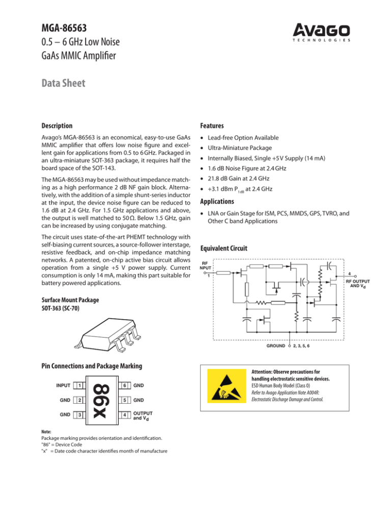
MGA-86563 0.5 – 6 GHz Low Noise GaAs MMIC Amplifier Data Sheet Description Features Avago’s MGA-86563 is an economical, easy-to-use GaAs MMIC amplifier that offers low noise figure and excellent gain for applications from 0.5 to 6 GHz. Packaged in an ultra-miniature SOT-363 package, it requires half the board space of the SOT-143. x Lead-free Option Available The MGA-86563 may be used without impedance matching as a high performance 2 dB NF gain block. Alternatively, with the addition of a simple shunt-series inductor at the input, the device noise figure can be reduced to 1.6 dB at 2.4 GHz. For 1.5 GHz applications and above, the output is well matched to 50 Ω. Below 1.5 GHz, gain can be increased by using conjugate matching. x 21.8 dB Gain at 2.4 GHz The circuit uses state-of-the-art PHEMT technology with self-biasing current sources, a source-follower interstage, resistive feedback, and on-chip impedance matching networks. A patented, on-chip active bias circuit allows operation from a single +5 V power supply. Current consumption is only 14 mA, making this part suitable for battery powered applications. x Ultra-Miniature Package x Internally Biased, Single +5 V Supply (14 mA) x 1.6 dB Noise Figure at 2.4 GHz x +3.1 dBm P1dB at 2.4 GHz Applications x LNA or Gain Stage for ISM, PCS, MMDS, GPS, TVRO, and Other C band Applications Equivalent Circuit RF NPUT 4 1 RF OUTPUT AND Vd Surface Mount Package SOT-363 (SC-70) GROUND Pin Connections and Package Marking 1 GND 2 GND 3 86x INPUT 6 GND 5 GND 4 OUTPUT and Vd Note: Package marking provides orientation and identification. "86" = Device Code "x" = Date code character identifies month of manufacture 2, 3, 5, 6 Attention: Observe precautions for handling electrostatic sensitive devices. ESD Human Body Model (Class 0) Refer to Avago Application Note A004R: Electrostatic Discharge Damage and Control. MGA-86563 Absolute Maximum Ratings Symbol Parameter Units Absolute Maximum[1] Vd Device Voltage, RF Output to Ground V 9 Vin RF Input Voltage to Ground V +0.5 –1.0 Pin CW RF Input Power dBm +13 Tch Channel Temperature °C 150 TSTG Storage Temperature °C -65 to 150 Thermal Resistance[2]:Tch-c = 160°C/W Notes: 1. Operation of this device above any one of these limits may cause permanent damage. 2. TC = 25°C (TC is defined to be the temperature at the package pins where contact is made to the circuit board). Electrical Specifications, TC = 25°C, ZO = 50 Ω unless noted, Vd = 5 V Symbol Parameters and Test Conditions Units Typ. 17 20 Gain in Test Circuit[1] f = 2.0 GHz NFtest Noise Figure in Test Circuit[1] f = 2.0 GHz NFO Optimum Noise Figure (Tuned for lowest noise figure) f = 0.9 GHz f = 2.0 GHz f = 2.4 GHz f = 4.0 GHz f = 6.0 GHz dB 2.0 1.5 1.6 1.7 2.0 GA Associated Gain at NFO (Tuned for lowest noise figure) f = 0.9 GHz f = 2.0 GHz f = 2.4 GHz f = 4.0 GHz f = 6.0 GHz dB 20.8 22.7 22.5 18.0 13.7 P1 dB Output Power at 1 dB Gain Compression (50 Ω Performance) f = 0.9 GHz f = 2.0 GHz f = 2.4 GHz f = 4.0 GHz f = 6.0 GHz dBm 3.6 4.1 4.2 4.3 3.3 IP3 Third Order Intercept Point f = 2.4 GHz dBm +15 VSWR in Input VSWR f = 2.4 GHz VSWRout Output VSWR f = 2.4 GHz Id Device Current 1.8 2.3:1 1.7:1 mA Note: 1. Guaranteed specifications are 100% tested in the circuit in Figure 10 in the Applications Information section. 2 Min. Gtest 14 Max. 2.3 MGA-86563 Typical Performance, TC = 25°C, Vd = 5 V 3 +85 +25 2 -40 1 25 20 1 2 3 4 5 -40 +25 +85 15 10 6 0 1 Figure 1. Minimum Noise Figure (Optimum Tuning) vs. Frequency and Temperature. 1 2 3 4 5 5 0 6 20 5.5 V 5.0 V 4.5 V 15 10 1 2 3 4 5 6 OUTPUT 1.5 0 1 5 6 FREQUENCY (GHz) Figure 7. Input and Output VSWR (into 50 Ω) vs. Frequency. 4 3 6 5 16 -40 +25 +50 +85 14 24 3.0 2.5 NF 50 2.0 1.5 16 NFopt 1.0 0 2 Figure 6. Output Power for 1 dB Gain Compression (into 50 Ω) vs. Frequency and Voltage. 32 GA 50 8 0.5 4 7.0 V 5.5 V 5.0 V 4.5 V 4 FREQUENCY (GHz) 12 CURRENT (mA) 2.0 3 6 0 0 ASSOCIATED GAIN (dB) NOISE FIGURE (dB) INPUT 2.5 6 5 2 5 3.5 3.0 4 3 Figure 3. Output Power for 1 dB Gain Compression (into 50 Ω) vs. Frequency and Temperature. Figure 5. Associated Gain (Optimum Tuning) vs. Frequency and Voltage. 3.5 2 8 4.0 2 1 FREQUENCY (GHz) 4.0 1 0 FREQUENCY (GHz) 25 0 6 Figure 4. Minimum Noise Figure (Optimum Tuning) vs. Frequency and Voltage. 0 -40 +25 +50 10 FREQUENCY (GHz) VSWR (n:1) 4 P 1 dB (dBm) 5.5 V 5.0 V 4.5 V 2 ASSOCIATED GAIN (dB) NOISE FIGURE (dB) 3 1 3 3 30 4 1.0 2 Figure 2. Associated Gain (Optimum Tuning) vs. Frequency and Temperature. 5 0 4 FREQUENCY (GHz) FREQUENCY (GHz) 0 6 2 +85 5 0 0 8 P 1 dB (dBm) ASSOCIATED GAIN (dB) NOISE FIGURE (dB) 4 0 10 30 5 10 8 6 4 2 0 2 4 6 8 10 0 12 FREQUENCY (GHz) Figure 8. 50 Ω Noise Figure and Associated Gain vs. Frequency. 0 0 1 2 3 4 5 VOLTAGE (V) Figure 9. Device Current vs. Voltage. 6 7 MGA-86563 Typical Scattering Parameters[1], TC = 25°C, ZO = 50 Ω, Vd = 5 V Freq. GHz Mag. S11 Ang. dB S21 Mag. Ang. dB S12 Mag. Ang. Mag. Ang. K Factor 0.1 0.5 1.0 1.5 2.0 2.5 3.0 3.5 4.0 4.5 5.0 5.5 6.0 6.5 7.0 7.5 8.0 0.84 0.57 0.55 0.53 0.47 0.38 0.26 0.14 0.04 0.04 0.07 0.09 0.11 0.12 0.13 0.15 0.17 -17 -29 -41 -57 -73 -89 -104 -115 -106 -6 2 -4 -17 -28 -36 -44 -53 3.1 14.7 18.9 20.8 21.7 21.8 21.3 20.2 18.8 17.4 16.1 14.9 13.9 12.9 12.0 11.1 10.4 1.42 5.41 8.77 10.97 12.14 12.33 11.61 10.23 8.75 7.44 6.41 5.57 4.93 4.40 3.96 3.58 3.30 76 41 4 -29 -62 -94 -125 -152 -177 162 143 126 110 94 79 65 51 -39.8 -44.3 -51.2 -52.1 -45.2 -40.7 -37.4 -34.4 -32.6 -30.9 -29.6 -28.1 -26.0 -24.9 -23.8 -22.6 -22.6 0.010 0.006 0.003 0.002 0.005 0.009 0.014 0.018 0.023 0.027 0.032 0.038 0.044 0.050 0.057 0.065 0.074 15 -23 -2 70 96 102 100 97 92 88 83 78 72 65 59 53 44 0.85 0.59 0.46 0.38 0.32 0.24 0.16 0.09 0.03 0.03 0.05 0.06 0.08 0.08 0.09 0.11 0.13 -15 -39 -53 -66 -78 -89 -99 -102 -82 1 20 19 14 4 -3 -12 -21 3.27 6.77 10.49 14.23 5.94 3.78 2.92 2.75 2.58 2.58 2.53 2.45 2.38 2.35 2.29 2.21 2.10 MGA-86563 Typical Noise Parameters[1], TC = 25°C, ZO = 50 Ω, Vd = 5 V Frequency (GHz) NFo (dB) Mag. Ang. RN/50 Ω 5 1.0 1.5 2.0 2.5 3.0 4.0 5.0 6.0 2.8 1.8 1.5 1.5 1.6 1.6 1.7 1.9 2.1 0.61 0.56 0.50 0.45 0.41 0.38 0.32 0.24 0.15 4 24 33 40 50 57 73 98 131 1.16 0.47 0.34 0.38 0.33 0.30 0.28 0.27 0.24 Note: 1. Reference plane per Figure 11 in Applications Information section. 4 S22 MGA-86563 Applications Information Introduction Biasing The MGA-86563 is a high gain, low noise RF amplifier for use in wireless RF applications within the 0.5 to 6 GHz frequency range. The MGA-86563 is a three-stage, GaAs Microwave Monolithic Integrated Circuit (MMIC) amplifier that uses internal feedback to provide wideband gain and impedance matching. The MGA-86563 is a voltage-biased device and operates from a single +5 volt power supply. With a typical current drain of only 14 mA, the MGA-86563 is suitable for use in battery powered applications. RF performance is very stable over a wide variation of power supply voltage. A patented, active bias circuit makes use of current sources to “re-use” the drain current in all three stages of gain, thus minimizing the required supply current and decreasing sensitivity to variations in power supply voltage. Test Circuit The circuit shown in Figure 10 is used for 100% RF testing of Noise Figure and Gain. The input of this circuit is fixed tuned for a conjugate power match (maximum power transfer, or, minimum Input VSWR) at 2 GHz. Tests in this circuit are used to guarantee the NFtest and Gtest parameters shown in the Electrical Specifications Table. The 3.3 nH inductor, L1 (Coilcraft, Cary, IL or equivalent) in series with the input of the amplifier matches the input to 50Ω at 2 GHz. Since DC bias is applied to the MGA-86563 through the RF Output pin, some method of isolating the RF from the DC must be provided. An RF choke or length of high impedance transmission line is typically used for this purpose. SOT-363 PCB Layout A PCB pad layout for the miniature SOT-363 (SC-70) package used by the MGA-86563 is shown in Figure 12 (dimensions are in inches). This layout provides ample allowance for package placement by automated assembly equipment without adding parasitics that could impair the high frequency RF performance of the MGA-86563. The layout is shown with a nominal SOT-363 package footprint superimposed on the PCB pads. The parameter test circuit uses a high impedance RF choke to apply Vd to the MMIC while isolating the power supply from the RF Output of the amplifier. w = 15 I = 1000 BOARD MATERIAL = 1/16" FR-4 w = 110 (50 Ω) RFC (28 nH) L1 3.3 nH RF INPUT Vd C1 w = 110 I = 110 w = 110 (50 Ω) RF OUTPUT Figure 10. Test Circuit for 2 GHz. Phase Reference Planes The positions of the reference planes used to measure SParameters and to specify*opt for the Noise Parameters are shown in Figure 11. As seen in the illustration, the reference planes are located at the extremities of the package leads. REFERENCE PLANES TEST CIRCUIT Figure 11. Reference Planes. 5 Figure 12. Recommended PCB Pad Layout for Avago’s SC70 6L/SOT-363 Products. RF Layout The RF layout in Figure 13 is suggested as a starting point for amplifier designs using the MGA-86563 MMIC. Adequate grounding is needed to obtain maximum performance and to obviate potential instability. All four ground pins of the MMIC should be connected to RF ground by using plated through holes (vias) near the package terminals. It is recommended that the PCB pads for the ground pins NOT be connected together underneath the body of the package. PCB traces hidden under the package cannot be adequately inspected for SMT solder quality. 50 Ω RF INPUT 86 50 Ω RF OUTPUT AND Vd Figure 13. RF Layout. PCB Material FR-4 or G-10 printed circuit board material is a good choice for most low cost wireless applications. Typical board thickness is 0.020 or 0.031 inches. The width of 50Ω microstriplines in PC boards of these thicknesses is also convenient for mounting chip components such as the series inductor that is used at the input for impedance matching or for DC blocking capacitors. For applications requiring the lowest noise figures, the use of PTFE/glass dielectric materials may be warranted to minimize transmission line losses at the amplifier input. A 0.5 inch length of 50Ω microstripline on FR-4 has approximately 0.3 dB loss at 4 GHz which will add directly to the noise figure of the MGA-86563. DC power is applied to the MMIC through the same pin that is shared with the RF output. A 50Ω microstripline is used to connect the device to the following stage. A bias decoupling network is used to feed in Vd while simultaneously providing a DC block to the RF signal. The bias decoupling network shown in Figure 14, consisting of resistor R1, a short length of high impedance microstripline, and bypass capacitor C3, will provide excellent performance over a wide frequency range. Surface mount chip inductors could be used in place of the high impedance transmission line to act as an RF choke. Consideration should be given to potential resonances and signal radiation when using lumped inductors. For operation at frequencies below approximately 2 GHz, the addition of a simple impedance matching circuit to the output will increase the gain and output power by 0.5 to 1.5 dB. The output matching circuit will not effect the noise figure. A small value resistor placed in series with the Vdd line may be useful to “de-Q” the bias circuit. Typical values of R1 are in the 10 Ω to 100 Ω range. Depending on the value of resistance used, the supply voltage may have to be increased to compensate for voltage drop across R1. The power supply should be capacitively bypassed (C3) to ground to prevent undesirable gain variations and to eliminate unwanted feedback through the bias lines that could cause oscillation. Vd C3 HIGH Z R1 C1 50 Ω C2 L1 50 Ω 50 Ω 50 Ω Typical Application Circuit A typical implementation of the MGA-86563 as a low noise amplifier is shown in Figure 14. A 50Ω microstripline with a series DC blocking capacitor, C1, is used to feed RF to the MMIC. The input of the MGA86563 is already partially matched for noise figure and gain to 50Ω. The use of a simple input matching circuit, such as a series inductor, will minimize amplifier noise figure. Since the impedance match for NFO (minimum noise figure) is very close to a conjugate power match, a low noise figure can be realized simultaneously with a low input VSWR. Figure 14. Typical Amplifier Circuit. Higher Bias Voltages While the MGA-86563 is designed primarily for use in +5 volt applications, the internal bias regulation circuitry allows it to be operated with any power supply voltage from +5 to +7 volts. The use of +7 volts increases the P1dB by approximately 1 dBm. The effect on noise figure, gain, and VSWR with higher Vd is negligible. For more information call your nearest Avago sales office. 6 Part Number Ordering Information No. of Devices Container MGA-86563-TR1 3000 7" Reel MGA-86563-TR2 10000 13" Reel MGA-86563-BLK 100 antistatic bag MGA-86563-TR1G 3000 7" Reel MGA-86563-TR2G 10000 13" Reel MGA-86563-BLKG 100 antistatic bag Part Number Note: For lead-free option, the part number will have the character “G” at the end. Package Dimensions Outline 63 (SOT-363/SC-70) HE E e D Q1 A2 A c A1 L b DIMENSIONS (mm) SYMBOL E D HE A A2 A1 Q1 e b c L 7 MIN. 1.15 1.80 1.80 0.80 0.80 0.00 0.10 0.650 BCS 0.15 0.10 0.10 MAX. 1.35 2.25 2.40 1.10 1.00 0.10 0.40 0.30 0.20 0.30 NOTES: 1. All dimensions are in mm. 2. Dimensions are inclusive of plating. 3. Dimensions are exclusive of mold flash & metal burr. 4. All specifications comply to EIAJ SC70. 5. Die is facing up for mold and facing down for trim/form, ie: reverse trim/form. 6. Package surface to be mirror finish. Device Orientation REEL TOP VIEW END VIEW 4 mm CARRIER TAPE 8 mm 86 86 86 86 USER FEED DIRECTION COVER TAPE Tape Dimensions and Product Orientation For Outline 63 P P2 D P0 E F W C D1 t1 (CARRIER TAPE THICKNESS) Tt (COVER TAPE THICKNESS) K0 10° MAX. 10° MAX. A0 DESCRIPTION B0 SYMBOL SIZE (mm) SIZE (INCHES) CAVITY LENGTH WIDTH DEPTH PITCH BOTTOM HOLE DIAMETER A0 B0 K0 P D1 2.40 ± 0.10 2.40 ± 0.10 1.20 ± 0.10 4.00 ± 0.10 1.00 + 0.25 0.094 ± 0.004 0.094 ± 0.004 0.047 ± 0.004 0.157 ± 0.004 0.039 + 0.010 PERFORATION DIAMETER PITCH POSITION D P0 E 1.55 ± 0.10 4.00 ± 0.10 1.75 ± 0.10 0.061 + 0.002 0.157 ± 0.004 0.069 ± 0.004 CARRIER TAPE WIDTH THICKNESS W t1 8.00 + 0.30 - 0.10 0.254 ± 0.02 0.315 + 0.012 0.0100 ± 0.0008 COVER TAPE WIDTH TAPE THICKNESS C Tt 5.40 ± 0.10 0.062 ± 0.001 0.205 + 0.004 0.0025 ± 0.0004 DISTANCE CAVITY TO PERFORATION (WIDTH DIRECTION) F 3.50 ± 0.05 0.138 ± 0.002 CAVITY TO PERFORATION (LENGTH DIRECTION) P2 2.00 ± 0.05 0.079 ± 0.002 For product information and a complete list of distributors, please go to our web site: www.avagotech.com Avago, Avago Technologies, and the A logo are trademarks of Avago Technologies in the United States and other countries. Data subject to change. Copyright © 2005-2010 Avago Technologies. All rights reserved. Obsoletes AV01-0199EN AV02-2514EN - October 27, 2010

