Understanding the ADS1252 Input Circuitry
advertisement
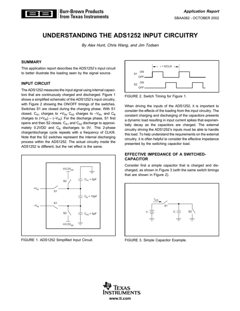
Application Report SBAA082 - OCTOBER 2002 UNDERSTANDING THE ADS1252 INPUT CIRCUITRY By Alex Hunt, Chris Wang, and Jim Todsen SUMMARY τ = 6/CLK This application report describes the ADS1252’s input circuit to better illustrate the loading seen by the signal source. S1 ON OFF INPUT CIRCUIT S2 The ADS1252 measures the input signal using internal capacitors that are continuously charged and discharged. Figure 1 shows a simplified schematic of the ADS1252’s input circuitry, with Figure 2 showing the ON/OFF timings of the switches. Switches S1 are closed during the charging phase. With S1 closed, CA1 charges to +VIN, CA2 charges to –VIN, and CB charges to (+VIN) – (–VIN). For the discharge phase, S1 first opens and then S2 closes. CA1 and CA2 discharge to approximately 0.2VDD and CB discharges to 0V. This 2-phase charge/discharge cycle repeats with a frequency of CLK/6. Note that the S2 switches represent the internal discharging process within the ADS1252. The actual circuitry inside the ADS1252 is different, but the net effect is the same. ON OFF FIGURE 2. Switch Timing for Figure 1. When driving the inputs of the ADS1252, it is important to consider the effects of the loading from the input circuitry. The constant charging and discharging of the capacitors presents a dynamic load resulting in input current spikes that exponentially decay as the capacitors are charged. The external circuitry driving the ADS1252’s inputs must be able to handle this load. To help understand the requirements on the external circuitry, it is often helpful to consider the effective impedance presented by the switching capacitor load. EFFECTIVE IMPEDANCE OF A SWITCHEDCAPACITOR Consider first a simple capacitor that is charged and discharged, as shown in Figure 3 (with the same switch timings that are shown in Figure 2). ≈ 0.2VDD S2 +VIN CA1 = 5pF S1 CB = 10pF –VIN IAVE S1 S1 S2 V CA2 = 5pF C ≈ 0.2VDD FIGURE 1. ADS1252 Simplified Input Circuit. FIGURE 3. Simple Capacitor Example. www.ti.com S2 The average current load of this signal (IAVE) is: IAVE ≡ f Q CV = = CV CLK t τ 6 (1) Defining the effective impedance as: Zeff ≡ V IAVE (2) and combining with Equation 1 results in: Zeff = 1 fCLK C 6 It is sometimes convenient to consider the input impedance with respect to the differential and common-mode voltages shown in Figure 5. Using ZDM (differential effective input impedance) and ZCM (common-mode effective input impedance), the input currents are: I+ = ZDMVDM + ZCM(VCM – 0.2VDD) (4) I– = –ZDMVDM + ZCM(VCM – 0.2VDD) (5) Referring to the circuit in Figure 4, it can be shown that: (3) ZDM = ZeffB 2ZeffAM (6) ZCM = ZeffA (7) EFFECTIVE INPUT CIRCUIT With the help of Equation 3, the circuitry to Figure 1 can be redrawn with effective impedances, as shown in Figure 4. Table I lists the impedances versus CLK frequency. VDM 2 – + I+ + – I– +VIN ≈ 0.2VDD ZeffA = 1 +VIN VCM ZeffB = –VIN (5pF)(CLK/6) VDM 2 1 (10pF)(CLK/6) –VIN ZeffA = 1 (5pF)(CLK/6) FIGURE 5. Differential and Common-Mode Signal Definitions. ≈ 0.2VDD FIGURE 4. Effective Input Impedances of the ADS1252. CLK FREQUENCY (MHz) ZeffA (kΩ) ZeffB (kΩ) 1 4 8 16 1200 300 150 75 600 150 75 37 CLK FREQUENCY (MHZ) ZDM (kΩ) ZCM (kΩ) 1 4 8 16 480 120 60 30 1200 300 150 75 TABLE II. Differential and Common-Mode Effective Input Impedances for Different CLK Frequencies. TABLE I. Effective Input Impedances for Different CLK Frequencies. 2 SBAA082 www.ti.com IMPORTANT NOTICE Texas Instruments Incorporated and its subsidiaries (TI) reserve the right to make corrections, modifications, enhancements, improvements, and other changes to its products and services at any time and to discontinue any product or service without notice. Customers should obtain the latest relevant information before placing orders and should verify that such information is current and complete. All products are sold subject to TI’s terms and conditions of sale supplied at the time of order acknowledgment. TI warrants performance of its hardware products to the specifications applicable at the time of sale in accordance with TI’s standard warranty. Testing and other quality control techniques are used to the extent TI deems necessary to support this warranty. Except where mandated by government requirements, testing of all parameters of each product is not necessarily performed. TI assumes no liability for applications assistance or customer product design. Customers are responsible for their products and applications using TI components. To minimize the risks associated with customer products and applications, customers should provide adequate design and operating safeguards. TI does not warrant or represent that any license, either express or implied, is granted under any TI patent right, copyright, mask work right, or other TI intellectual property right relating to any combination, machine, or process in which TI products or services are used. Information published by TI regarding third–party products or services does not constitute a license from TI to use such products or services or a warranty or endorsement thereof. Use of such information may require a license from a third party under the patents or other intellectual property of the third party, or a license from TI under the patents or other intellectual property of TI. Reproduction of information in TI data books or data sheets is permissible only if reproduction is without alteration and is accompanied by all associated warranties, conditions, limitations, and notices. Reproduction of this information with alteration is an unfair and deceptive business practice. TI is not responsible or liable for such altered documentation. Resale of TI products or services with statements different from or beyond the parameters stated by TI for that product or service voids all express and any implied warranties for the associated TI product or service and is an unfair and deceptive business practice. TI is not responsible or liable for any such statements. Mailing Address: Texas Instruments Post Office Box 655303 Dallas, Texas 75265 Copyright 2002, Texas Instruments Incorporated
