Flip flops
advertisement

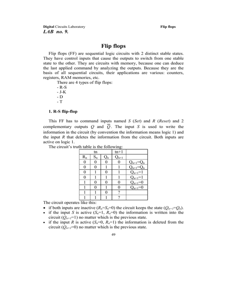
Digital Circuits Laboratory Flip flops LAB no. 9. Flip flops Flip flops (FF) are sequential logic circuits with 2 distinct stable states. They have control inputs that cause the outputs to switch from one stable state to the other. They are circuits with memory, because one can deduce the last applied command by analyzing the outputs. Because they are the basis of all sequential circuits, their applications are various: counters, registers, RAM memories, etc. There are 4 types of flip flops: - R-S - J-K -D -T 1. R-S flip-flop This FF has to command inputs named S (Set) and R (Reset) and 2 complementary outputs Q and Q . The input S is used to write the information in the circuit (by convention the information means logic 1) and the input R that deletes the information from the circuit. Both inputs are active on logic 1. The circuit’s truth table is the following: tn tn+1 Rn Sn Qn Qn+1 0 0 0 0 Qn+1=Qn 0 0 1 1 Qn+1=Qn 0 1 0 1 Qn+1=1 0 1 1 1 Qn+1=1 1 0 0 0 Qn+1=0 1 0 1 0 Qn+1=0 1 1 0 ? 1 1 1 ? The circuit operates like this: if both inputs are inactive (Rn=Sn=0) the circuit keeps the state (Qn+1=Qn). if the input S is active (Sn=1, Rn=0) the information is written into the circuit (Qn+1=1) no matter which is the previous state. if the input R is active (Sn=0, Rn=1) the information is deleted from the circuit (Qn+1=0) no matter which is the previous state. 49 Digital Circuits Laboratory Flip flops LAB no. 9. the case Rn=Sn=1 has no sense, because is not logic to write and to delete the information in the same moment. The good working condition for this circuit is RnSn=0. Above, tn is the actual moment, and Rn, Sn, Qn are the input and the output values at the present moment, and tn+1 is the next moment, Qn+1 is the output in this moment. For the circuit synthesis Qn+1 is considered output signal. The Karnaugh diagrams for the outputs are the following: SnRn 00 01 11 10 0 0 0 X 1 1 1 0 X 1 Qn SnRn 00 01 11 10 0 1 1 X 0 1 0 1 X 0 Qn Qn 1 S n Qn Rn Qn 1 Rn Qn S n For the synthesis, the de Morgan theorem will be used in order to implement the circuit with NAND gates only: Qn1 Q n1 ( S n Qn Rn ) S n ( Qn Rn ) Q n1 Q n1 ( Rn Qn S n ) Rn ( Qn S n ) Thus, the circuit looks like in the next figure: S R S Q Q R The circuit has the inputs active on logic 1. If the inverters are taken out, the circuit will have the inputs active on logic 0. The above circuit can be implemented with NOR gates only. For this we will group the cells containing logic 0: 50 Digital Circuits Laboratory Flip flops LAB no. 9. SnRn 00 01 11 10 0 0 0 X 1 1 1 0 X 1 Qn SnRn 00 01 11 10 0 1 1 X 0 1 0 1 X 0 Qn Qn 1 ( S n Qn ) Rn Qn 1 ( Rn Qn ) S n Applying the de Morgan theorem the equations become: Qn 1 Q n1 ( S n Qn ) Rn ( Qn S n ) Rn Q n 1 Q n 1 ( Rn Q n ) S n ( Q n Rn ) S n In this case the circuit will look like in the following figure: S Q Q R The above circuit is an asynchronous one. The synchronous circuit is also available. It has the inputs activated by a clock signal (following figure). As long as T is logic 0, the AND gates have the outputs in logic 0 no matter which are the inputs R and S. In these conditions its state cannot be changed. When T is logic 1 then R’=R and S’=S and the circuit works like in the asynchronous version. S S’ Q T R’ Q R 2. J-K flip flop This kind of flip flop eliminates the RS flip flop indefinite state. It has 2 51 Digital Circuits Laboratory Flip flops LAB no. 9. inputs J and K and a clock input in the synchronous version. a) Asynchronous J-K flip flop The truth table of this circuit is the following: tn tn+1 Jn Kn Qn Qn+1 0 0 0 0 Qn+1=Qn 0 0 1 1 Qn+1=Qn 0 1 0 0 Qn+1=0 0 1 1 0 Qn+1=0 1 0 0 1 Qn+1=1 1 0 1 1 Qn+1=1 1 1 0 1 Qn+1=Qn 1 1 1 0 Qn+1= Qn The input J has the same role as the input S for the R-S flip flop and the input K as R. The difference is for J=K=1 when instead of the indefinite state the output switches to the complementary one. The VK associated diagrams are: JnKn 00 01 11 10 0 0 0 1 1 1 1 0 0 1 Qn Qn 1 J n Qn Qn K n JnKn 00 01 11 10 0 1 1 0 0 1 0 1 1 0 Qn Qn 1 K n Qn Qn J n The above equations can be rewritten: Qn1 Q n1 K n Qn Qn J n Qn Q n1 Qn1 K n Qn Q n J n Qn The flip flop looks like: K S Q Q J R 52 Digital Circuits Laboratory Flip flops LAB no. 9. The block framed in the dotted square is a R-S flip flop. We can deduce immediately the connection equation between the two flip flops: Rn J n Qn S n K n Qn Another implementation choice that comes from the above equations is the following: Rn K n Qn , S n J n Qn and has the next schematic: J K S Q Q R b) Synchronous J-K flip flop The synchronous J-K flip flops are obtained by replacing the 2 inputs NAND gates cu 3 input gates, the clock being connected to the third: K S J Q T S T Q R J Q Q K R Their disadvantage is that for T=1 the circuit oscillates. c) Master-slave J-K flip flop In order to eliminate the oscillation a master slave structure has been proposed. This is based on two pipelined J-K flip flops. The first flip flop (the master) stores the data on the positive edge of the clock signal T, while the second (slave) is detached. When the clock T is logic 0, the data is 53 Digital Circuits Laboratory Flip flops LAB no. 9. transferred from master to slave, while the master is detached from the inputs. In the following figure it is shown the logic schematic of this circuit. S S’ J S” Q J S Q Ck K R Q Ck Ck K Q’ J R’ R” Q Q’ K R The truth table associated with the master –slave flip flop is: Jn 0 0 1 1 Kn 0 1 0 1 Qn+1 Qn 0 1 Qn Ck The symbol „” signify the fact that the output changes on the negative edge of the clock signal. 3. T flip flop In many applications the JK flip flop is used with the inputs connected at logic 1. This connection represents another type of flip flop: T flip flop or counting cell. Its truth table is: T Ck Qn+1 0 Qn 1 Qn 54 Digital Circuits Laboratory Flip flops LAB no. 9. The flip flop realizes the clock frequency division with 2. As long as T=1, the output changes its state every two clock transitions (every negative edge). This property makes it suitable for using in counter’s construction. T T Ck t J S Q Ck K R Q Ck t Q t 4. D flip flop D R Q Ck S Q This circuit has an input called D (data) and a clock input (Ck). Besides these, it has two asynchronous inputs R and S that have the highest priority. The value at the input at tn goes at the output at tn+1, as we can notice from its truth table. tn+1 tn D Qn Qn+1 0 0 0 0 1 0 1 0 1 1 1 1 From the truth table we observe that Qn+1=Dn. Thus, the D flip flop introduces a delay of the input state. The output at the moment tn+1 is the 55 Digital Circuits Laboratory Flip flops LAB no. 9. same as the input at the tn (delay cell or memory cell). This circuit is useful for realizing static RAM memories, registers but also counters. Generally, any type of flip flop can be replaced with other type using conversion schemes. 3. Lab work Print the Lab sheet below and complete it according to the indications. 56 Digital Circuits Laboratory Flip flops LAB no. 9. LAB SHEET 1. Input the RS flip flop with NAND gates in MaxPlusII and simulate the circuit. Draw the waveforms from the simulation on the grid below. Write the delay time and the logic values on the waveforms. Compare the results with the truth table. Introduce the inverters on the inputs, save as a new circuit and simulate again. Draw the waveforms in this case. S S R R Q Q Q Q 2. Input in MaxPlusII a JK flip flop (JKFF from the library) and simulate it. Draw the waveforms on the grid below, measure the delay and compare the results with the truth table. clk J K Q Q 3. Input a D flip flop (DFF in the library) and simulate it. Draw the waveforms below, measure the delay and compare the results with the truth table. clk D Q Q 57


