UJT Characteristics: Lab Experiment
advertisement
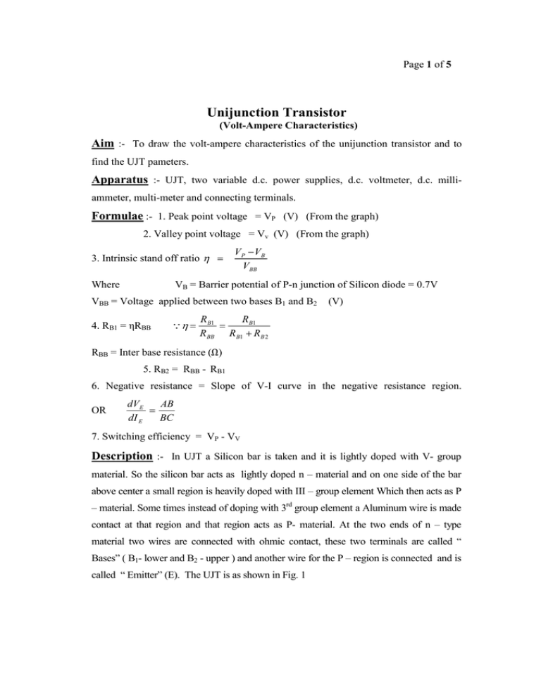
Page 1 of 5 Unijunction Transistor (Volt-Ampere Characteristics) Aim :- To draw the volt-ampere characteristics of the unijunction transistor and to find the UJT pameters. Apparatus :- UJT, two variable d.c. power supplies, d.c. voltmeter, d.c. milliammeter, multi-meter and connecting terminals. Formulae :- 1. Peak point voltage = VP (V) (From the graph) 2. Valley point voltage = Vv (V) (From the graph) 3. Intrinsic stand off ratio η = Where V P − VB VBB VB = Barrier potential of P-n junction of Silicon diode = 0.7V VBB = Voltage applied between two bases B1 and B2 4. RB1 = ηRBB Qη = (V) R B1 R B1 = R BB R B1 + RB 2 RBB = Inter base resistance (Ω) 5. RB2 = RBB - RB1 6. Negative resistance = Slope of V-I curve in the negative resistance region. OR dVE AB = dI E BC 7. Switching efficiency = VP - VV Description :- In UJT a Silicon bar is taken and it is lightly doped with V- group material. So the silicon bar acts as lightly doped n – material and on one side of the bar above center a small region is heavily doped with III – group element Which then acts as P – material. Some times instead of doping with 3rd group element a Aluminum wire is made contact at that region and that region acts as P- material. At the two ends of n – type material two wires are connected with ohmic contact, these two terminals are called “ Bases” ( B1- lower and B2 - upper ) and another wire for the P – region is connected and is called “ Emitter” (E). The UJT is as shown in Fig. 1 Page 2 of 5 Fig. 1 Fig. 2 Since the Silicon bar is lightly doped, the resistance between the bases B2 and B1 is high and its value ranges from 5 KΩ to 10 KΩ at room temperature. This is called ‘double base diode’. If some potential is applied between the bases B2 and B1, a uniform potential gradient is developed between them. Because of its resistance this will also acts as a potential divider and this divides the potential at E. In this UJT it has only one P-n junction, so it is called unijunction transistor. ( Since it has three terminals it acts as transistor.) The circuit symbol of UJT is as shown in the fig. 2. The arrowed terminal is the emitter and it gives the conventional current direction. The emitter arrow is inclined towards the base B1 terminal because in the ‘conducting state’ the current will flow from emitter to base B1. Fig. 3 Page 3 of 5 THEORY :- Case 1:- First the emitter (E) is open i.e. it is given zero potential and a fixed voltage ‘VBB’ is applied between two bases B1 and B2, such that B2 is given positive that is B2 is at +VBB and B1 is at zero potential. This VBB produces a current from B2 to B1, which in turn produces a uniform potential gradient between B2 and B1, as the Silicon bar has a resistance of 5 KΩ to 10 KΩ. The potential at the point ‘A’ in the Silicon bar, where the emitter region touches the n-type bar is ‘ηVBB’, where η is the intrinsic stand off ratio or ‘voltage division factor’. The emitter is open means it is given zero potential then the P-n junction is reverse biased, and the current through the junction is zero. Case 2:- Now a variable voltage VE from a source VEE is applied between the emitter E and base B1 When VE is less than ‘ηVBB’ then the P-n junction is reverse biased and the resistance between A and B1 i.e. RB1 is high. In this stage a small reverse leakage current will flow B2 to E. When VE exceeds ηVBB then the junction is for ward biased, but when VE ≥ ηVBB + VB, holes enter from emitter ‘E’ to the n-type bar and these are repelled by the base B2 due to its positive potential and are attracted by B1 which is at negative potential. ( Actually these holes get neutralized by attracting electrons from B1, here VB is the potential barrier of P-n junction). So the conductivity of this part of bar ( A to B1) increases and the resistance RB1 decreases. i.e. The emitter current IE causes a decrease in the resistance which is known as negative resistance characteristic. In this stage emitter voltage VE also decreases to a low value corresponding to the decrease of resistance RB1. This minimum voltage is called the ‘valley point voltage’ VV and the corresponding current is called ‘valley point current’ IV. The emitter voltage is maximum when VE = ηVBB + VB and is called ‘peak point’ voltage (VP) or ‘firing potential’. The current corresponding to VP is called ‘peak point current’ IP. Above IV the VE increases gradually and this state is called ‘on-state’ and the corresponding region in the graph is called ‘saturation region’. Page 4 of 5 Fig. 4 Procedure :- First the emitter is open and the inter base resistance ‘RBB’ is measured with a ohmmeter. Now the circuit is connected as shown in Fig.3. Apply a fixed voltage VBB (5V to 10V) between the two bases B1 and B2. Increase the emitter voltage VE in convenient steps starting from zero. Note the corresponding emitter current IE. Draw a graph by taking IE on X-axis and VE on Y-axis. The shape of the graph is as shown in the Fig. 4. Note the peak point P and valley point V also note the corresponding voltages VP & VV and currents IP & IV. Find the value of intrinsic stand off ratio η, switching efficiency (VP - VV), RB1and RB2 using the above formulae. Also find the value of the negative resistance of UJT from the slope drawn to the curve in the –ve resistance region. The characteristic curves can be drawn with different values of VBB. The VP and VV values increase with the increasing value of VBB. The IP and IV values do not change with the change of VBB.The switching efficiency also increases with increasing value of VBB. Page 5 of 5 Graph-1 :- A graph is drawn by taking emitter current IE on X-axis and emitter Voltage VE on Y-axis. From the graph the VP and VV values and IP and IV values are noted as shown in the graph Fig. 4. Precautions :- 1) The continuity of the connecting terminals should be checked before going to connect the circuit. 2) Identify the two bases and emitter of UJT and connect properly. 3) The power supply should be ‘on’ only when the observations are taken. Table S. No. VBB = Volt IE (mA) VE (Volt) ***** VBB = Volt IE (mA) VE (Volt)
