Capacitance and Resistance Model Capacitance Any two
advertisement
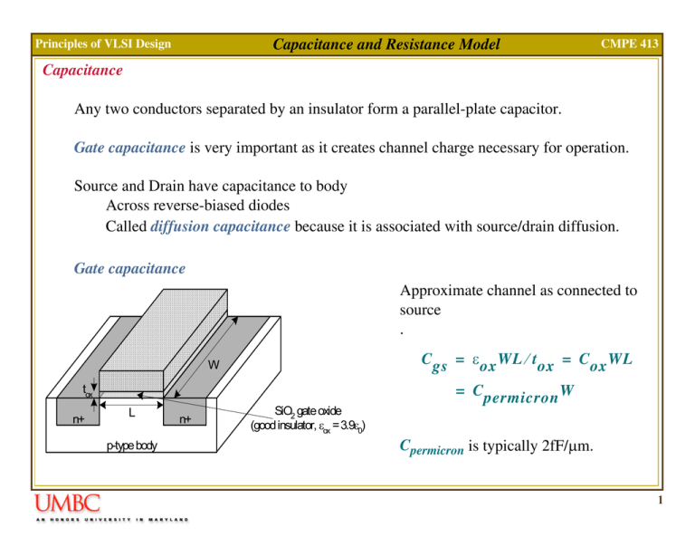
Capacitance and Resistance Model Principles of VLSI Design CMPE 413 Capacitance Any two conductors separated by an insulator form a parallel-plate capacitor. Gate capacitance is very important as it creates channel charge necessary for operation. Source and Drain have capacitance to body Across reverse-biased diodes Called diffusion capacitance because it is associated with source/drain diffusion. Gate capacitance Approximate channel as connected to source . polysilicon gate C gs = ε ox WL ⁄ t ox = C ox WL W tox n+ L p-type body n+ SiO2 gate oxide (good insulator, εox = 3.9ε0) = C permicron W Cpermicron is typically 2fF/µm. 1 Principles of VLSI Design Capacitance and Resistance Model CMPE 413 Diffusion Capacitance Csb, Cdb Undesirable, called parasitic capacitance. Capacitance depends on area and perimeter Use small diffusion nodes Comparable to Cg for contacted diffusion Half of Cg for uncontacted diffusion. Varies with process 2 Capacitance and Resistance Model Principles of VLSI Design CMPE 413 Gate Capacitance Details The gate capacitance can be decomposed into several parts: One part contributes to the channel charge. A second part is due to the topological structure of the transistor. MOS Structure Capacitances, Overlap: poly source n+ xd W drain n+ xd tox n+ Poly Leff n+ L Lateral diffusion: source and drain diffusion extend under the oxide by an amount xd. The effective channel length (Leff) is less than the drawn length L by 2*xd. This gives rise to a linear, fixed capacitance called overlap capacitance. C gsO = C gdO = C ox x d W = C O W Since xd is technology dependent, it is usually combined with Cox. 3 Principles of VLSI Design Capacitance and Resistance Model CMPE 413 Gate Capacitance Details Channel Charge The gate-to-channel capacitance is composed of three components, Cgs, Cgd and Cgb. Each of these is non-linear and dependent on the region of operation. Estimates or average values are often used Linear: Cgb ~=0 since the inversion region shields the bulk electrode from the gate. Saturation: Cgb and Cgd is ~= 0 since the channel is pinched off. Operation Region Cgb Cgs Cgd Cutoff CoxWLeff 0 0 Linear 0 CoxWLeff/2 CoxWLeff/2 Saturation 0 (2/3)CoxWLeff 0 4 Capacitance and Resistance Model Principles of VLSI Design CMPE 413 Diffusion Capacitance Details Junction or Diffusion Capacitances This component is caused by the reverse-biased source-bulk and drain-bulk pn-junctions. This capacitance is non-linear and decreases as reverse-bias is increased. sidewall channel-stop implant NA+ xj W ND Bottom channel sidewall LS Bottom-plate junction Depletion region capacitance is C bottom = C j WL S 5 Principles of VLSI Design Capacitance and Resistance Model CMPE 413 Diffusion Capacitance Details Cj is the junction capacitance per unit area. − Mj V sb⎞ ⎛ C j = C j0 ⎜ 1 + ---------⎟ Ψ0 ⎠ ⎝ where, Cj0 is the junction capacitance at zero bias and is highly process dependent. Mj is the junction grading coefficient, typically between 0.5 and 0.33 depending on the abruptness of the diffusion junction. Ψ0 is the built-in potential that depends on doping levels given by ⎛N N ⎞ A D Ψ 0 = υ T ln ⎜ -----------------⎟ ⎜ 2 ⎟ N ⎝ i ⎠ where, υT is the thermal voltage. NA and ND are doping levels of the body and source diffusion region. Ni is the intrinsic carrier concentration in undoped silicon. 6 Capacitance and Resistance Model Principles of VLSI Design CMPE 413 Diffusion Capacitance Details Side-Wall Capacitance Formed by the source region with doping ND and the p+channel-stop implant with doping NA+. Since the channel-stop doping is usually higher than the substrate, this results in a higher unit capacitance: C sw = C′ jsw x j ( W + 2 × L S ) C'jsw is similar to Cj but with different coefficients.Mj = 0.33 to 0.5. Note that the channel side is not included in the calculation. Some SPICE models have an extra parameter to account for this junction. xj is usually technology dependent and combined with C'jsw as Cjsw. Total diffusion/junction capacitance is: C diff = C bottom + C sw = C j × AREA + C jsw × PERIMETER C diff = C j L S W + C jsw ( 2L S + W ) 7 Capacitance and Resistance Model Principles of VLSI Design CMPE 413 MOS Capacitance Model Capacitive Device Model The previous model can be summarized as: G CGS CGD D S CSB CGB CDB CGS = Cgs + CgsO CGD = Cgd + CgdO CGB = Cgb CSB = CSdiff CDB = CDdiff B The dynamic performance of digital circuits is directly proportional to these capacitances! 8 Capacitance and Resistance Model Principles of VLSI Design CMPE 413 Source-Drain Resistance Scaling causes junctions to be shallower and contact openings to be smaller. This increases the parasitic resistance in series with the source and drain regions: G Gate VGS,eff LD Drain contact D S RS W RD Drain This resistance can be expressed as: L S, D R S, D = -------------- R W + RC R C = Contact Resistance = Sheet resistance ( 50Ω − 1kΩ ) R LS,D = length of source/drain region. The series resistance degrades device performance by decreasing drain current. One option is to cover drain and source regions with a low-resistivity material such as titanium or tungsten. This process is called silicidation, and is used in reducing poly resistance as well. 9 Principles of VLSI Design Capacitance and Resistance Model CMPE 413 Capacitance Example Given: t ox = 20nm L = 1.2um W = 1.8um L D = L S = 3.6um x d = 0.15um 2 F⁄m − 10 C jsw0 = 8 × 10 F⁄m Determine the zero-bias value of all relevant capacitances. Gate capacitance, Cox, per unit area is derived as: −2 2 3.5 × 10 fF ⁄ um C ox = ε ox ⁄ t ox = ---------------------------------------------- = 1.75fF ⁄ um −3 20 ×10 um Total gate capacitance Cg is: 2 C g = WLC ox = 1.8um × 1.2um × 1.75fF ⁄ um = 3.78fF C j0 = 3 × 10 −4 Overlap capacitance is: C GSO = C GDO = Wx d C ox = 0.47fF Subtracting out overlap capacitance yields Cgb under zero-bias: C gb = C ox WL eff = 3.78 − 2 × 0.47 = 2.84fF 10 Principles of VLSI Design Capacitance and Resistance Model CMPE 413 Capacitance Example Diffusion capacitance is the sum of bottom: −1 2 C j0 L D W = 3 ×10 fF ⁄ um × 3.6um × 1.8um = 1.95fF Plus side-wall (under zero-bias): −1 C jsw0 ( 2L D + W ) = 8 ×10 ( 2 × 3.6um + 1.8um ) = 7.2fF In this example, diffusion capacitance dominates gate capacitance (3.78fF versus 9.2fF). Note that this is the worst case condition. Increasing reverse bias reduces diffusion capacitance (by about 50%). Also note that side-wall dominates diffusion. Advanced processes use SiO2 to isolate devices (trench isolation) instead of NA+ implant. 11
