A simple, low-cost, versatile charge-coupled device spectrometer for
advertisement

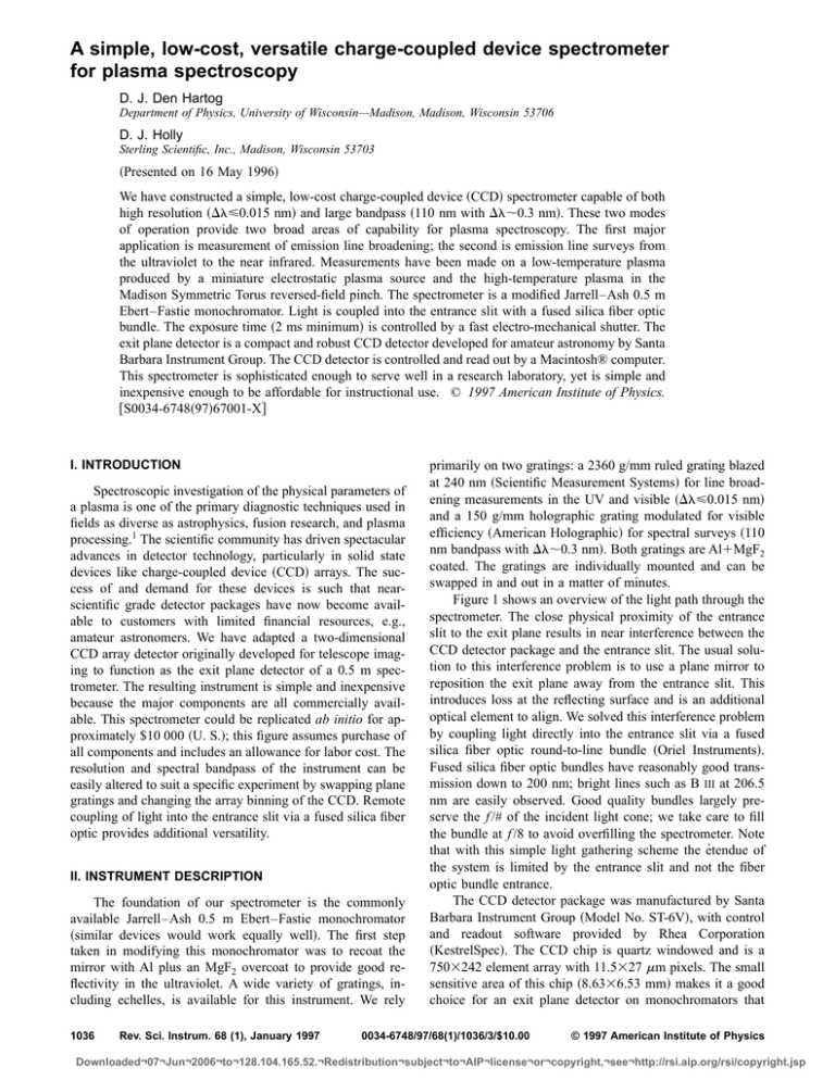
A simple, low-cost, versatile charge-coupled device spectrometer for plasma spectroscopy D. J. Den Hartog Department of Physics, University of Wisconsin—Madison, Madison, Wisconsin 53706 D. J. Holly Sterling Scientific, Inc., Madison, Wisconsin 53703 ~Presented on 16 May 1996! We have constructed a simple, low-cost charge-coupled device ~CCD! spectrometer capable of both high resolution ~Dl<0.015 nm! and large bandpass ~110 nm with Dl;0.3 nm!. These two modes of operation provide two broad areas of capability for plasma spectroscopy. The first major application is measurement of emission line broadening; the second is emission line surveys from the ultraviolet to the near infrared. Measurements have been made on a low-temperature plasma produced by a miniature electrostatic plasma source and the high-temperature plasma in the Madison Symmetric Torus reversed-field pinch. The spectrometer is a modified Jarrell–Ash 0.5 m Ebert–Fastie monochromator. Light is coupled into the entrance slit with a fused silica fiber optic bundle. The exposure time ~2 ms minimum! is controlled by a fast electro-mechanical shutter. The exit plane detector is a compact and robust CCD detector developed for amateur astronomy by Santa Barbara Instrument Group. The CCD detector is controlled and read out by a Macintosh® computer. This spectrometer is sophisticated enough to serve well in a research laboratory, yet is simple and inexpensive enough to be affordable for instructional use. © 1997 American Institute of Physics. @S0034-6748~97!67001-X# I. INTRODUCTION Spectroscopic investigation of the physical parameters of a plasma is one of the primary diagnostic techniques used in fields as diverse as astrophysics, fusion research, and plasma processing.1 The scientific community has driven spectacular advances in detector technology, particularly in solid state devices like charge-coupled device ~CCD! arrays. The success of and demand for these devices is such that nearscientific grade detector packages have now become available to customers with limited financial resources, e.g., amateur astronomers. We have adapted a two-dimensional CCD array detector originally developed for telescope imaging to function as the exit plane detector of a 0.5 m spectrometer. The resulting instrument is simple and inexpensive because the major components are all commercially available. This spectrometer could be replicated ab initio for approximately $10 000 ~U. S.!; this figure assumes purchase of all components and includes an allowance for labor cost. The resolution and spectral bandpass of the instrument can be easily altered to suit a specific experiment by swapping plane gratings and changing the array binning of the CCD. Remote coupling of light into the entrance slit via a fused silica fiber optic provides additional versatility. II. INSTRUMENT DESCRIPTION The foundation of our spectrometer is the commonly available Jarrell–Ash 0.5 m Ebert–Fastie monochromator ~similar devices would work equally well!. The first step taken in modifying this monochromator was to recoat the mirror with Al plus an MgF2 overcoat to provide good reflectivity in the ultraviolet. A wide variety of gratings, including echelles, is available for this instrument. We rely 1036 Rev. Sci. Instrum. 68 (1), January 1997 primarily on two gratings: a 2360 g/mm ruled grating blazed at 240 nm ~Scientific Measurement Systems! for line broadening measurements in the UV and visible ~Dl<0.015 nm! and a 150 g/mm holographic grating modulated for visible efficiency ~American Holographic! for spectral surveys ~110 nm bandpass with Dl;0.3 nm!. Both gratings are Al1MgF2 coated. The gratings are individually mounted and can be swapped in and out in a matter of minutes. Figure 1 shows an overview of the light path through the spectrometer. The close physical proximity of the entrance slit to the exit plane results in near interference between the CCD detector package and the entrance slit. The usual solution to this interference problem is to use a plane mirror to reposition the exit plane away from the entrance slit. This introduces loss at the reflecting surface and is an additional optical element to align. We solved this interference problem by coupling light directly into the entrance slit via a fused silica fiber optic round-to-line bundle ~Oriel Instruments!. Fused silica fiber optic bundles have reasonably good transmission down to 200 nm; bright lines such as B III at 206.5 nm are easily observed. Good quality bundles largely preserve the f /# of the incident light cone; we take care to fill the bundle at f /8 to avoid overfilling the spectrometer. Note that with this simple light gathering scheme the étendue of the system is limited by the entrance slit and not the fiber optic bundle entrance. The CCD detector package was manufactured by Santa Barbara Instrument Group ~Model No. ST-6V!, with control and readout software provided by Rhea Corporation ~KestrelSpec!. The CCD chip is quartz windowed and is a 7503242 element array with 11.5327 mm pixels. The small sensitive area of this chip ~8.6336.53 mm! makes it a good choice for an exit plane detector on monochromators that 0034-6748/97/68(1)/1036/3/$10.00 © 1997 American Institute of Physics Downloaded¬07¬Jun¬2006¬to¬128.104.165.52.¬Redistribution¬subject¬to¬AIP¬license¬or¬copyright,¬see¬http://rsi.aip.org/rsi/copyright.jsp FIG. 1. The light path through the spectrometer. The CCD detector package is shown without the mount. were not specifically designed to have a large flat exit focal plane. The CCD array is two stage thermoelectrically cooled, typically operating at 220 °C with gentle forced air circulation around the detector cooling fins. A variety of resolution modes are provided by combinations of hardware and software pixel binning; the two most useful ‘‘pixel sizes’’ for spectroscopy are 2336534 mm ~37531 array elements! and 11.536534 mm ~75031 array elements!. According to the manufacture’s specifications, typical dark current for a 23 36534 mm ‘‘pixel’’ is 3200 electrons/s with a rms readout noise of 110 electrons. For short exposures, the resulting noise fluctuations limit the dynamic range to about 12 bits even though the actual detector A/D is 16 bits. The maximum framing rate is limited to about 1 frame/s by the serial readout of the detector ~the detector controller connects to the serial port of the Macintosh!. Minimum integration time allowed by the detector package is 10 ms. We have reduced this to 2 ms by shuttering the entrance of the fiber optic input bundle with a fast electro-mechanical shutter ~Vincent Associates!. This CCD detector has been mounted on short focal length monochromators,2 but such adapters were not transferable to our 0.5 m monochromator and did not offer the fine positioning necessary to achieve the spectral resolution we needed. Our solution is shown in exploded view in Fig. 2. Final fine focus of the detector position is provided by adjustment of the translation stage. Perpendicularity of the detector plane to the optical axis is adjusted by shimming the stage mount. Note also that provision for vertical, horizontal, and rotational adjustment of the entrance slit is provided. FIG. 2. A detailed scaled perspective drawing of the CCD detector mount. Rev. Sci. Instrum., Vol. 68, No. 1, January 1997 FIG. 3. A single pixel instrument function for the Cd II 214.4 nm line with 10 mm entrance slit, 2360 g/mm grating, and 11.5 mm wide pixel. ‘‘Measured’’ is the actual instrument function measured by sweeping the 214.4 nm across the detector pixel; ‘‘predicted’’ is the design instrument function, including diffraction effects; ‘‘Gaussian’’ is a Gaussian function with FWHM of 0.0125 nm. Pixel to pixel spacing is 0.0093 nm. Alignment and calibration of the spectrometer is straightforward, following the commonly accepted techniques usually spelled out in the manual provided by the manufacturer of the monochromator. The two-dimensional FIG. 4. ~a! An impurity spectrum from the plasma inside the miniature electrostatic plasma source; the B III line brightness was purposefully enhanced by exposing boron nitride to the plasma. ~b! Broadening of the B III line ~206.5 nm! from the plasma source. Statistical ~Poisson! error bars are smaller than the cross used to mark the data points. Plasma diagnostics 1037 Downloaded¬07¬Jun¬2006¬to¬128.104.165.52.¬Redistribution¬subject¬to¬AIP¬license¬or¬copyright,¬see¬http://rsi.aip.org/rsi/copyright.jsp imaging capability of the CCD detector simplifies final fine adjustments; the goal is to image the entrance slit on a single vertical row of pixels. We have achieved near diffractionlimited performance with our instrument; an example instrument function is shown in Fig. 3. This trace was made by slowly scanning the Cd II 214.4 nm line across the exit plane and repeatedly reading out the CCD. The grating was driven by an inexpensive synchronous clock motor with appropriate gear reduction. The measured instrument function is fit fairly well by a Gaussian with a FWHM of 0.0125 nm; the pixelto-pixel spacing is 0.0093 nm. Also shown in Fig. 3 is the design instrument function calculated by convolving the results of geometric raytracing with the 11.5 mm wide square detector function and the expected diffraction sinc function.3 The agreement of the design and measured instrument function illustrates the good focus achieved with our CCD detector mount. ments have been made with the 2360 g/mm grating; Fig. 4~b! shows a typical measurement of the BIII line ~206.5 nm! from the plasma source. The Gaussian function fit to the data indicates a Doppler T i ~Ref. 5! of 14.7 eV; this ion temperature is in substantial agreement with the electron temperature derived from Langmuir probe measurements. The versatility of this spectrometer is illustrated by the fact that it is now being used to examine the high-temperature plasma in the Madison Synchrotron Torus reversed-field pinch, measuring the Doppler broadening and shift to determine the temperature and flow velocity of various impurity species. ACKNOWLEDGMENTS The authors thank D. Craig and G. Fiskel for assistance with the acquisition of the impurity and line broadening spectra. This work was supported by the United States Department of Energy. III. DIAGNOSTIC APPLICATIONS Our major applications of this spectrometer have been impurity surveys and line broadening. A representative impurity spectrum from a miniature electrostatic plasma source,4 using the 150 g/mm grating, is shown in Fig. 4~a!. Note that lines are clearly resolved across the entire spectrum, indicating good exit plane focus across the sensitive area of the detector. Successful line broadening measure- 1038 Rev. Sci. Instrum., Vol. 68, No. 1, January 1997 1 See, for example, the review of fusion spectroscopy in N. J. Peacock, UKAEA Report No. FUS 312 ~1995!. 2 J. O’Donnell, Scientific Measurement Systems ~private communication!. 3 F. A. Jenkins and H. E. White, Fundamentals of Optics, 4th ed. ~McGraw– Hill, New York, 1976!, p. 324. 4 G. Fiksel, A. F. Almagri, D. Craig, M. Iida, S. C. Prager, and J. S. Sarff, Plasma Sources Sci. Technol. 5, 78 ~1996!. 5 I. H. Hutchinson, Principles of Plasma Diagnostics ~Cambridge University Press, Cambridge, 1987!, pp. 216 –222. Plasma diagnostics Downloaded¬07¬Jun¬2006¬to¬128.104.165.52.¬Redistribution¬subject¬to¬AIP¬license¬or¬copyright,¬see¬http://rsi.aip.org/rsi/copyright.jsp


