Package Information for Arria GX Devices
advertisement
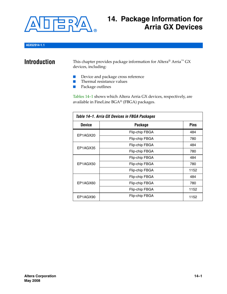
14. Package Information for Arria GX Devices AGX52014-1.1 Introduction This chapter provides package information for Altera® Arria™ GX devices, including: ■ ■ ■ Device and package cross reference Thermal resistance values Package outlines Tables 14–1 shows which Altera Arria GX devices, respectively, are available in FineLine BGA® (FBGA) packages. Table 14–1. Arria GX Devices in FBGA Packages Device EP1AGX20 EP1AGX35 EP1AGX50 EP1AGX60 EP1AGX90 Altera Corporation May 2008 Package Pins Flip-chip FBGA 484 Flip-chip FBGA 780 Flip-chip FBGA 484 Flip-chip FBGA 780 Flip-chip FBGA 484 Flip-chip FBGA 780 Flip-chip FBGA 1152 Flip-chip FBGA 484 Flip-chip FBGA 780 Flip-chip FBGA 1152 Flip-chip FBGA 1152 14–1 Introduction Thermal Resistance Thermal resistance values for Arria GX devices are provided for a board that meets JDEC specifications and for a typical board. The following values are provided: ■ ■ ■ ■ ■ ■ θJA (°C/W) still air—Junction-to-ambient thermal resistance with no air flow when a heat sink is not used. θJA (°C/W) 100 ft./min.—Junction-to-ambient thermal resistance with 100 ft./min. airflow when a heat sink is not used. θJA (°C/W) 200 ft./min.—Junction-to-ambient thermal resistance with 200 ft./min. airflow when a heat sink is not used. θJA (°C/W) 400 ft./min.—Junction-to-ambient thermal resistance with 400 ft./min. airflow when a heat sink is not used. θJC—Junction-to-case thermal resistance for device. θJB—Junction-to-board thermal resistance for device. Table 14–2 provides θ JA (junction-to-ambient thermal resistance), θJC (junction-to-case thermal resistance), and θJB (junction-to-board thermal resistance) values for Arria GX devices. Table 14–2. Arria GX GX Device Thermal Resistance Device Pin Count Package θJA (° C/W) Still Air θJA (° C/W) 100 ft./min. EP1AGX20 484 FBGA 12.8 10.3 8.7 7.5 0.3 3.14 780 FBGA 11.1 8.6 7.2 6.0 0.24 3.14 484 FBGA 12.8 10.3 8.7 7.5 0.3 3.14 780 FBGA 11.1 8.6 7.2 6.0 0.24 3.14 484 FBGA 12.7 10.2 8.6 7.3 0.2 2.86 780 FBGA 10.9 8.4 6.9 5.8 0.15 2.84 EP1AGX35 EP1AGX50 EP1AGX60 EP1AGX90 θJA (° C/W) θJA (° C/W) θJC θJB 200 ft./min. 400 ft./min. (° C/W) (° C/W) 1152 FBGA 9.9 7.5 6.1 5.0 0.15 2.5 484 FBGA 12.7 10.2 8.6 7.3 0.2 2.86 780 FBGA 10.9 8.4 6.9 5.8 0.15 2.84 1152 FBGA 9.9 7.5 6.1 5.0 0.15 2.5 1152 FBGA 9.6 7.3 5.9 4.9 0.11 2.33 This chapter contains the following section: ■ “Package Outlines” on page 14–3 14–2 Arria GX Device Handbook, Volume 2 Altera Corporation May 2008 Package Information for Arria GX Devices Package Outlines The package outlines are listed in order of ascending pin count. Altera package outlines meet the requirements of JEDEC Publication No. 95. 484-Pin FBGA - Flip Chip ■ ■ ■ All dimensions and tolerances conform to ASME Y14.5M – 1994. Controlling dimension is in millimeters. Pin A1 may be indicated by an ID dot, or a special feature, in its proximity on the package surface. Tables 14–3 and 14–4 show the package information and package outline figure references, respectively, for the 484-pin FBGA packaging. Table 14–3. 484-Pin FBGA Package Information Description Specification Ordering code reference F Package acronym FBGA Substrate material BT Solder ball composition Regular: 63Sn:37Pb (Typ.) Pb-free: Sn:3Ag:0.5Cu (Typ.) JEDEC outline reference MS-034 variation: AAJ-1 Maximum lead coplanarity 0.008 inches (0.20 mm) Weight 7.1 g Moisture sensitivity level Printed on moisture barrier bag Table 14–4. 484-Pin FBGA Package Outline Dimensions (Part 1 of 2) Millimeter Symbol Altera Corporation May 2008 Min. Nom. Max. A – – 3.50 A1 0.30 – – A2 0.25 – 3.00 A3 – – 2.50 D 23.00 BSC E 23.00 BSC 14–3 Arria GX Device Handbook, Volume 2 Package Outlines Table 14–4. 484-Pin FBGA Package Outline Dimensions (Part 2 of 2) Millimeter Symbol b Min. Nom. Max. 0.50 0.60 0.70 e 1.00 BSC Figure 14–1 shows a package outline for the 484-pin FineLine BGA packaging. Figure 14–1. 484-Pin FBGA Package Outline TOP VIEW BOTTOM VIEW Pin A1 Corner D Pin A1 ID e E b e A A2 A3 A1 14–4 Arria GX Device Handbook, Volume 2 Altera Corporation May 2008 Package Information for Arria GX Devices 780-Pin FBGA - Flip Chip ■ ■ ■ Arria GX Device Handbook, Volume 2All dimensions and tolerances conform to ASME Y14.5M - 1994. Controlling dimension is in millimeters. Pin A1 may be indicated by an ID dot, or a special feature, in its proximity on package surface. Tables 14–5 and 14–6 show the package information and package outline figure references, respectively, for the 780-pin FBGA packaging. Table 14–5. 780-Pin FBGA Package Information Description Specification Ordering code reference F Package acronym FBGA Substrate material BT Solder ball composition Regular: 63Sn:37Pb (Typ.) Pb-free: Sn:3Ag:0.5Cu (Typ.) JEDEC outline reference MS-034 Maximum lead coplanarity 0.008 inches (0.20 mm) Weight 11.9 g Moisture Sensitivity Level Printed on moisture barrier bag variation: AAM-1 Table 14–6. 780-Pin FBGA Package Outline Dimensions Millimeters Symbol A Min. Nom. Max. – – 3.50 A1 0.30 – – A2 0.25 – 3.00 A3 – – 2.50 D 29.00 BSC E b e Altera Corporation May 2008 29.00 BSC 0.50 0.60 0.70 1.00 BSC 14–5 Arria GX Device Handbook, Volume 2 Package Outlines Figure 14–2 shows a package outline for the 780-pin FineLine BGA packaging. Figure 14–2. 780-Pin FBGA Package Outline TOP VIEW BOTTOM VIEW D Pin A1 Corner Pin A1 ID e E b e A A2 A3 A1 14–6 Arria GX Device Handbook, Volume 2 Altera Corporation May 2008 Package Information for Arria GX Devices 1,152-Pin FBGA - Flip Chip ■ ■ ■ All dimensions and tolerances conform to ASME Y14.5M - 1994. Controlling dimension is in millimeters. Pin A1 may be indicated by an ID dot, or a special feature, in its proximity on package surface. Tables 14–7 and 14–8 show the package information and package outline figure references, respectively, for the 1,152-pin FBGA packaging. Table 14–7. 1,152-Pin FBGA Package Information Description Specification Ordering code reference F Package acronym FBGA Substrate material BT Solder ball composition Regular: 63Sn:37Pb (Typ.) Pb-free: Sn:3Ag:0.5Cu (Typ.) JEDEC outline reference MS-034 Maximum lead coplanarity 0.008 inches (0.20 mm) Weight 15.8 g Moisture sensitivity level Printed on moisture barrier bag variation: AAR-1 Table 14–8. 1,152-Pin FBGA Package Outline Dimensions Millimeters Symbol Min. Nom. Max. A – – 3.50 A1 0.30 – – A2 0.25 – 3.00 A3 – – 2.50 D 35.00 BSC E 35.00 BSC b e Altera Corporation May 2008 0.50 0.60 0.70 1.00 BSC 14–7 Arria GX Device Handbook, Volume 2 Document Revision History Figure 14–3 shows a package outline for the 1,152-pin FineLine BGA packaging. Figure 14–3. 1,152-Pin FBGA Package Outline TOP VIEW BOTTOM VIEW D Pin A1 Corner Pin A1 ID e E b e A A2 A3 A1 Document Revision History Table 14–9 shows the revision history for this document. Table 14–9. Document Revision History Date and Document Version Changes Made May 2007, v1.1 Minor text edits. May 2007, v1.0 Initial Release 14–8 Arria GX Device Handbook, Volume 2 Summary of Changes — N/A Altera Corporation May 2008
