PN Junction Reverse Bias: Depletion Region & Capacitance
advertisement

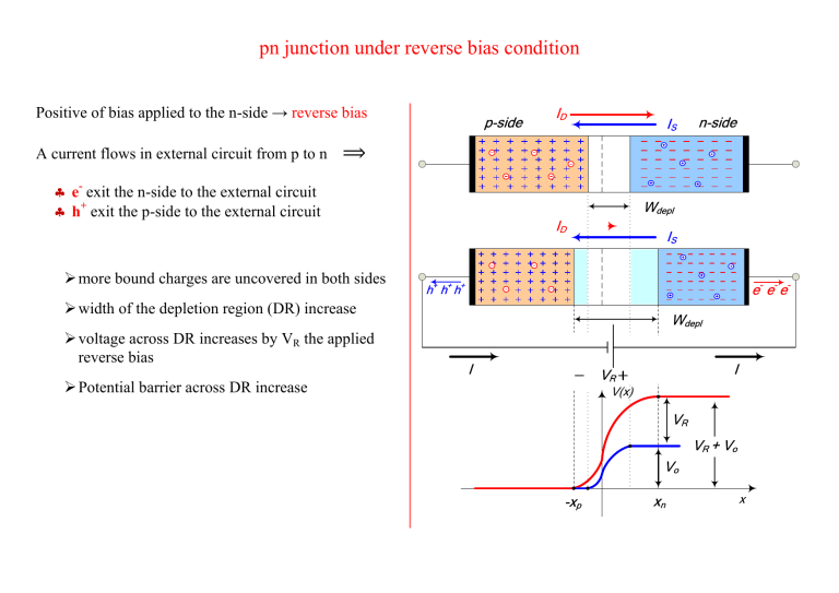
pn junction under reverse bias condition Positive of bias applied to the n-side → reverse bias A current flows in external circuit from p to n p-side ID IS n-side ⟹ e- exit the n-side to the external circuit h+ exit the p-side to the external circuit more bound charges are uncovered in both sides Wdepl ID IS e- e - e- h+ h+ h+ width of the depletion region (DR) increase voltage across DR increases by VR the applied reverse bias Wdepl I I VR Potential barrier across DR increase V(x) VR VR + Vo Vo -xp xn x Diffusion current ID decrease to zero ( it depends on barrier) Drift current IS remain unchanged (it does not dependent on barrier) The total reverse current at equilibrium (steady state) is given by: 𝐼 = 𝐼𝑆 − 𝐼𝐷 ≅ 𝐼𝑆 This current flows in the external circuit from p to n. inside the junction the current flows from n to p ( same as IS) Since the reverse current is equal to IS it is independent of the reverse bias applied: reverse current is constant it depends on temperature Depletion capacitance width of SCL changes with applied reverse bias ⟹ +qj and -qj charges stored at both side of junction change with bias ⟹ pn junction behaves like a capacitor This is similar to a capacitor: An expression for qj is: 𝑞𝑗 = 𝑞𝑁𝐷 𝑥𝑛 𝐴 ; A ≡ cross sectional area of the junction 𝑊𝑑𝑒𝑝𝑙 = 𝑥𝑛 + 𝑥𝑝 and To get qj in terms of Wdepl, as: Where Wdepl is given by: 𝑥𝑝 = qj 𝑁𝐴 𝑁𝐷 𝑞𝑗 = 𝑞𝐴 𝑁 𝐴 𝑁𝐷 𝑁𝐴 +𝑁𝐷 𝑊𝑑𝑒𝑝𝑙 2 s 1 1 (V0 VR ) wdepl q N A ND 𝑞𝑗 = 𝐴 2𝑞𝜀𝑠 𝑁𝐴 𝑁𝐷 (𝑉 + 𝑉𝑅 ) 𝑁𝐴 + 𝑁𝐷 𝑜 Charge stored in Depl. Region Use: 𝑥𝑛 Slope = Cj Q Bias Point VQ Reverse voltage VR Curve of stored charge qj versus applied reverse bias VR. → qj Capacitor is not constant, it depends on the bias point "Depletion capacitance" or "Junction capacitance" is the slope of qj – VR curve at the bias point Q: 𝐶𝑗 = 𝑑𝑞 𝑗 𝑑𝑉𝑅 𝑉𝑅 =𝑉𝑄 = 𝜀𝑠 𝐴 𝑊 𝑑𝑒𝑝𝑙 Where Cj0 is the value of Cj at VR = 0: 𝐶𝑗 0 ; 𝐶𝑗 = 𝐶𝑗 0 𝑉 1+ 𝑅 𝑉𝑜 =𝐴 𝑞𝜀 𝑠 𝑁𝐴 𝑁𝐷 2 𝑁𝐴 +𝑁𝐷 Charge stored in Depl. Region qj – VR is nonlinear Slope = Cj Q Bias Point VQ 1 ( ) 𝑉𝑜 Reverse voltage VR 𝐶𝑗 0 𝐶𝑗 = 𝑉 1+ 𝑅 𝑉𝑜 𝑚


