3.15: Transistors in ‘forward active’ mode Common base circuit
advertisement
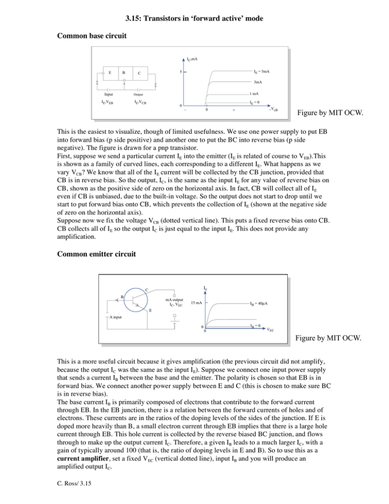
3.15: Transistors in ‘forward active’ mode Common base circuit IC,mA E B IE = 5mA 5 C 3mA Input 1 mA Output IE,VEB IE,VCB 0 IE = 0 _ 0 _V + cB Figure by MIT OCW. This is the easiest to visualize, though of limited usefulness. We use one power supply to put EB into forward bias (p side positive) and another one to put the BC into reverse bias (p side negative). The figure is drawn for a pnp transistor. First, suppose we send a particular current IE into the emitter (IE is related of course to VEB).This is shown as a family of curved lines, each corresponding to a different IE. What happens as we vary VCB? We know that all of the IE current will be collected by the CB junction, provided that CB is in reverse bias. So the output, IC, is the same as the input IE for any value of reverse bias on CB, shown as the positive side of zero on the horizontal axis. In fact, CB will collect all of IE even if CB is unbiased, due to the built-in voltage. So the output does not start to drop until we start to put forward bias onto CB, which prevents the collection of IE (shown at the negative side of zero on the horizontal axis). Suppose now we fix the voltage VCB (dotted vertical line). This puts a fixed reverse bias onto CB. CB collects all of IE so the output IC is just equal to the input IE. This does not provide any amplification. Common emitter circuit Ic C B E mA output IC, VEC 15 mA IB = 40µA A input 0 0 IB = 0 VEC Figure by MIT OCW. This is a more useful circuit because it gives amplification (the previous circuit did not amplify, because the output IC was the same as the input IE). Suppose we connect one input power supply that sends a current IB between the base and the emitter. The polarity is chosen so that EB is in forward bias. We connect another power supply between E and C (this is chosen to make sure BC is in reverse bias). The base current IB is primarily composed of electrons that contribute to the forward current through EB. In the EB junction, there is a relation between the forward currents of holes and of electrons. These currents are in the ratios of the doping levels of the sides of the junction. If E is doped more heavily than B, a small electron current through EB implies that there is a large hole current through EB. This hole current is collected by the reverse biased BC junction, and flows through to make up the output current IC. Therefore, a given IB leads to a much larger IC, with a gain of typically around 100 (that is, the ratio of doping levels in E and B). So to use this as a current amplifier, set a fixed VEC (vertical dotted line), input IB and you will produce an amplified output IC. C. Ross/ 3.15
