Carrier Transport: Drift
advertisement
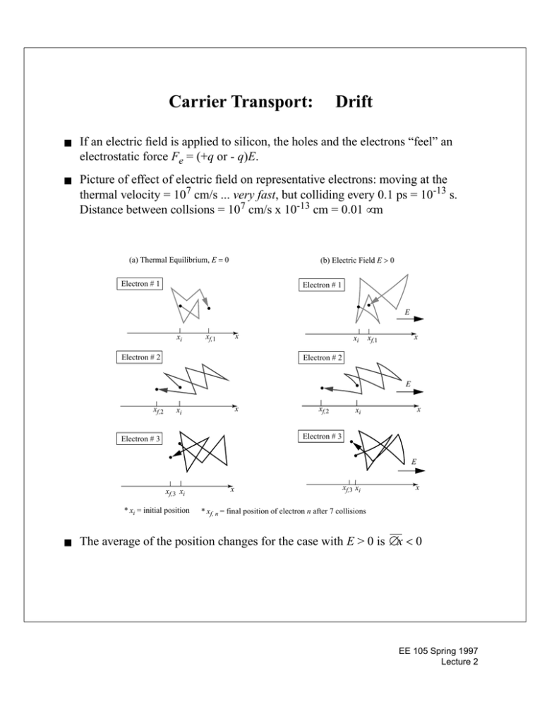
Carrier Transport: Drift ■ If an electric field is applied to silicon, the holes and the electrons “feel” an electrostatic force Fe = (+q or - q)E. ■ Picture of effect of electric field on representative electrons: moving at the thermal velocity = 107 cm/s ... very fast, but colliding every 0.1 ps = 10-13 s. Distance between collsions = 107 cm/s x 10-13 cm = 0.01 µm (a) Thermal Equilibrium, E = 0 (b) Electric Field E > 0 Electron # 1 Electron # 1 E xi x xf,1 Electron # 2 xi x xf,1 Electron # 2 E xf,2 x xi xf,2 x xi Electron # 3 Electron # 3 E xf,3 xi * xi = initial position ■ x xf,3 xi x * xf, n = final position of electron n after 7 collisions The average of the position changes for the case with E > 0 is ∆x < 0 EE 105 Spring 1997 Lecture 2 Drift Velocity and Mobility ■ The drift velocity vdn of electrons is defined as: ∆x v dn = -----∆t ■ Experiment shows that the drift velocity is proportional to the electric field for electrons v dn = – µ n E , with the constant µn defined as the electron mobility. ■ Holes drift in the direction of the applied electric field, with the constant µp defined as the hole mobility. v dp = µ p E How do we know what’s positive and what’s negative? positive: E negative: E x x EE 105 Spring 1997 Lecture 2 Electron and Hole Mobilities ■ mobilities vary with doping level -- plot is for 300 K = room temp. 1400 1200 electrons mobility (cm2/Vs) 1000 800 600 holes 400 200 0 1013 ■ 1014 1015 1016 1017 1018 Nd + Na total dopant concentration (cm−3) 1019 1020 “typical values” for bulk silicon - assuming around 5 x 1016 cm-3 doping µn = 1000 cm2/(Vs) µp = 400 cm2/(Vs) ■ at electric fields greater than around 104 V/cm, the drift velocities saturate --> max. out at around 107 cm/s. Velocity saturation is very common in VLSI devices, due to sub-micron dimensions EE 105 Spring 1997 Lecture 2 Carrier Transport: Drift Current Density Electrons drifting opposite to the electric field are carrying negative charge; therefore, the drift current density is: Jndr = (-q) n vdn units: Ccm-2 s-1 = Acm-2 Jndr = (-q) n (- µn E) = q n µn E Note that Jndr is in the same direction as the electric field. For holes, the mobility is µp and the drift velocity is in the same direction as the electric field: vdp = µp E The hole drift current density is: Jpdr = (+q) p vdp Jpdr = q p µp E EE 105 Spring 1997 Lecture 2 Drift Current Directions and Signs ■ For electrons, an electric field in the +x direction will lead to a drift velocity in the -x direction (vdn < 0) and a drift current density in the +x direction (Jndr > 0). electron drift current density Jndr vdn E x ■ For holes, an electric field in the +x direction will lead to a drift velocity in the +x direction (vdp >0) and a drift current density in the +x direction (Jndr > 0). hole drift current density Jpdr vdp E x EE 105 Spring 1997 Lecture 2 Carrier Transport: Diffusion Diffusion is a transport process driven by gradients in the concentration of particles in random motion and undergoing frequent collisions -- such as ink molecules in water ... or holes and electrons in silicon. Mathematics: find the number of carriers in a volume Aλ on either side of the reference plane, where λ is the mean free path between collisions. ■ Some numbers: average carrier velocity = vth = 107 cm/s, average interval between collisions = τc = 10-13 s = 0.1 picoseconds mean free path = λ = vth τc = 10-6 cm = 0.01 µm reference plane (area = A) p(x) hole diffusion Jpdiff (positive) p(xr − λ) volume Aλ: holes moving in + x direction cross reference plane within ∆t = τc. p(xr + λ) xr − λ ■ xr xr + λ volume Aλ: holes moving in − x direction cross reference plane within ∆t = τc. x half of the carriers in each volume will pass through the plane before their next collision, since their motion is random EE 105 Spring 1997 Lecture 2 Carrier Transport: Diffusion Current Density ■ Current density = (charge) x (# carriers per second per area): 1 1 --- p ( x – λ ) Aλ – --- p( x + λ) Aλ diff 2 2 J p = q ---------------------------------------------------------------------Aτ c ■ If we assume that λ is much smaller than the dimensions of our device, then we can consider λ = dx and use Taylor expansions : diff Jp = – qD p dp , dx where Dp = λ2 / τc is the diffusion coefficent EE 105 Spring 1997 Lecture 2 Electron Transport by Diffusion ■ Electrons diffuse down the concentration gradient, yet carry negative charge --> electron diffusion current density points in the direction of the gradient n(x) Jndiff ( < 0) Jndiff ( > 0) x ■ Total current density: add drift and diffusion components for electrons and for holes -dr diff dn = qnµ n E + qD n dx dr diff dp = qpµ p E – qD p dx Jn = Jn + Jn Jp = Jp + Jp ■ Fortunately, we will be able to eliminate one or the other component in finding the internal currents in microelectronic devices. EE 105 Spring 1997 Lecture 2 Carrier Transport by Diffusion ■ Holes diffuse “down” the concentration gradient and carry a positive charge --> hole diffusion current has the opposite sign to the gradient in hole concentration dp/dx p(x) Jpdiff ( > 0) Jpdiff ( < 0) x ■ Electrons diffuse down the concentration gradient, yet carry a negative charge --> electron diffusion current density has the same sign as the gradient in electron concentration dn/ dx. n(x) Jndiff ( < 0) Jndiff ( > 0) x EE 105 Spring 1997 Lecture 2 Electron Diffusion Current Density ■ Similar analysis leads to diff Jn dn = qD n ------ , dx where Dn is the electron diffusion coefficient (units: cm2/s) ■ Numerical values of diffusion coefficients: use Einstein’s relation Dn kT ------- = -----µn q ■ The quantity kT/q has units of volts and is called the thermal voltage, Vth: kT V th = ------ = 25 – 26 mV, q at “room temperature,” with 25 mV for a cool room (62 oF) and 26 mV for a warm room (83 oF). We will pick 25 mV or 26 mV depending on which gives the “roundest” numbers. EE 105 Spring 1997 Lecture 2 Total Current Densities ■ Add drift and diffusion components for electrons and for holes -- dr diff dn = qnµ n E + qD n dx dr diff dp = qpµ p E – qD p dx Jn = Jn + Jn Jp = Jp + Jp ■ Fortunately, we will be able to eliminate one or the other component of the electron or the hole current in our analysis of semiconductor devices. EE 105 Spring 1997 Lecture 2 IC Fabrication Technology ■ History: 1958-59: J. Kilby, Texas Instruments and R. Noyce, Fairchild 1959-70: Explosive growth in US (bipolar ICs) 1970-85: MOS ICs introduced, RAMs, microprocessors, Japan catches up to US in volume 1985-95: PC revolution, improved design software for complex CMOS integrated systems, US leads in microprocessors, Japan in RAMs 1996-2000 > 108 devices/chip ( = 1000 Mbit dRAM), US remains competitive -- even dominates -- sectors of the market; spin-offs from IC technology in MEMS (micro electromechanical systems) for sensing acceleration ■ Key Idea: batch fabrication of electronic circuits An entire circuit, say 106 transistors and associated wiring -- can be made in and on top of a single silicon crystal by a series of process steps similar to printing. The silicon crystal is a thin disk about the size of a small dinner plate (ca. 1996) called a wafer. More than 100 copies of the circuit are made at the same time. ■ Results: 1. Complex systems can be fabricated reliably 2. Cost per function drops as the process improves (e.g., finer printing), since the cost per processed wafer remains about the same EE 105 Spring 1997 Lecture 2 Photolithography ■ The essential process step: makes possible the transfer of a series of patterns onto the wafer -- all aligned to within 0.1 µm ■ Process “Tool” -- wafer stepper ultraviolet light illumination field area is opaque mask lens wafer scan direction exposed dice ■ unexposed dice region of silicon wafer (coated with photoresist) UV-sensitive film is called photoresist. Regions exposed to UV dissolve in developer (for positive photoresist -- the type we will consider) EE 105 Spring 1997 Lecture 2 Exposure, Development, and Pattern Transfer ■ Simple example of a layout and a process (or recipe) * Layout is the set of mask patterns for particular layers (one in this case) * Process is the sequence of fabrication steps ■ Visualize by generating cross sections through the structure as it is built up through the process A A Mask Pattern B B 0 1 2 3 4 5 6 x (µm) EE 105 Spring 1997 Lecture 2
