Enhanced Endurance Performance of 0.13µm Ramtron Nonvolatile
advertisement

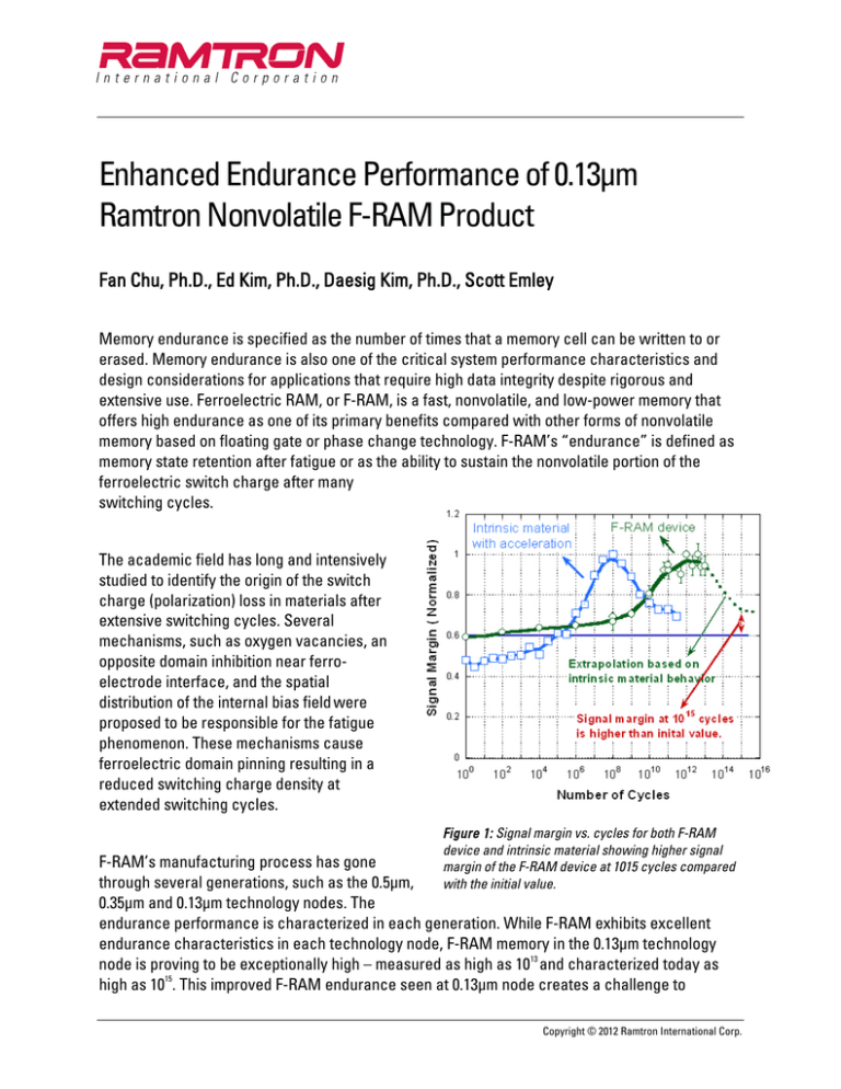
Enhanced Endurance Performance of 0.13µm Ramtron Nonvolatile F-RAM Product Fan Chu, Ph.D., Ed Kim, Ph.D., Daesig Kim, Ph.D., Scott Emley Memory endurance is specified as the number of times that a memory cell can be written to or erased. Memory endurance is also one of the critical system performance characteristics and design considerations for applications that require high data integrity despite rigorous and extensive use. Ferroelectric RAM, or F-RAM, is a fast, nonvolatile, and low-power memory that offers high endurance as one of its primary benefits compared with other forms of nonvolatile memory based on floating gate or phase change technology. F-RAM’s “endurance” is defined as memory state retention after fatigue or as the ability to sustain the nonvolatile portion of the ferroelectric switch charge after many switching cycles. The academic field has long and intensively studied to identify the origin of the switch charge (polarization) loss in materials after extensive switching cycles. Several mechanisms, such as oxygen vacancies, an opposite domain inhibition near ferroelectrode interface, and the spatial distribution of the internal bias field were proposed to be responsible for the fatigue phenomenon. These mechanisms cause ferroelectric domain pinning resulting in a reduced switching charge density at extended switching cycles. Figure 1: Signal margin vs. cycles for both F-RAM device and intrinsic material showing higher signal margin of the F-RAM device at 1015 cycles compared with the initial value. F-RAM’s manufacturing process has gone through several generations, such as the 0.5µm, 0.35µm and 0.13µm technology nodes. The endurance performance is characterized in each generation. While F-RAM exhibits excellent endurance characteristics in each technology node, F-RAM memory in the 0.13µm technology node is proving to be exceptionally high – measured as high as 1013 and characterized today as 15 high as 10 . This improved F-RAM endurance seen at 0.13µm node creates a challenge to 1 Copyright © 2012 Ramtron International Corp. Enhanced Endurance Performance of 0.13µm Ramtron Nonvolatile F-RAM Product measure the actual maximum endurance behavior in a reasonable amount of time (Table1). Extensive test time and innovative test methodologies are needed to determine the actual endurance limit of 0.13µm F-RAM product. Table 1: Time to exercise 1 Byte parallel F-RAM. Number of endurance cycles Cycle Time Days 1010 1012 1014 1015 0.025 2.55 255 2550 The current endurance specification of 1015 cycles for 0.13µm F-RAM is based on the preliminary evaluation of 1,280 bits of F-RAM memory from a sample of Ramtron parallel F-RAM core memory products built using the 0.13µm technology node. Figure 1 shows that the device level signal margin reaches maximum between 1012 and 1013 cycles. Based on the endurance behavior of the intrinsic material for 0.13µm F-RAM (shown in Figure 1), the device level endurance behavior post 1013 cycles can be extrapolated using similar curve observed in intrinsic material as shown in dashed line in Figure 1. It can be seen that the remaining signal margin after 1015 cycles is still higher than the initial level (the signal margin at minimum number of cycles), indicating that there is enough signal margin to ensure the reliability of F-RAM device after 1015 cycles. This result is consistent with the endurance specification of the 0.13µm F-RAM foundry and the specification of Ramtron’s respective products. 2 Copyright © 2012 Ramtron International Corp. Enhanced Endurance Performance of 0.13µm Ramtron Nonvolatile F-RAM Product Conclusion When determining whether an F-RAM product is an appropriate solution for a given application, system designers should consider the following: • Is the system designed to collect data? • Does the configuration change often? • Can power fail suddenly or frequently? • Is the data highly valuable? • Is power supply noisy? • Is there a need to capture critical system data during power down, which will enable a graceful system recovery on power up? • Is memory endurance vital for storing mission critical data? • Is the system or MCU RAM-limited? • Is there a strict power budget? In such cases, F-RAM’s technical features can reduce operational overhead and ensure optimal performance. For more information You can find out more about how F-RAM semiconductor products can improve your next system design via the following resources: • For general information, visit www.ramtron.com • To order a product sample, visit www.ramtron.com/sales/order-samples.aspx. • To contact your local authorized sales representative, visit www.ramtron.com/sales/buy-now.aspx • Call Customer Service at 719-481-7181, or email info@ramtron.com About Ramtron International Corporation Ramtron International Corporation, headquartered in Colorado Springs, Colorado, is a fabless semiconductor company that designs, develops, and markets specialized semiconductor memory and integrated semiconductor solutions used in a wide range of product applications and markets worldwide. For more information, visit www.ramtron.com. Ramtron International Corporation, 1850 Ramtron Drive, Colorado Springs, CO 80921. 3 Copyright © 2012 Ramtron International Corp.


