Compact SiC Power Module for High Speed Switching
advertisement
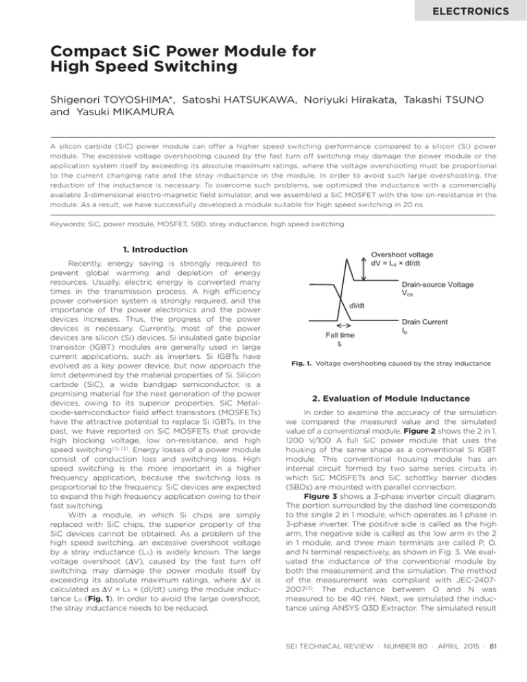
ELECTRONICS Compact SiC Power Module for High Speed Switching Shigenori TOYOSHIMA*, Satoshi HATSUKAWA, Noriyuki Hirakata, Takashi TSUNO and Yasuki MIKAMURA ---------------------------------------------------------------------------------------------------------------------------------------------------------------------------------------------------------------------------------------------------------A silicon carbide (SiC) power module can offer a higher speed switching performance compared to a silicon (Si) power module. The excessive voltage overshooting caused by the fast turn off switching may damage the power module or the application system itself by exceeding its absolute maximum ratings, where the voltage overshooting must be proportional to the current changing rate and the stray inductance in the module. In order to avoid such large overshooting, the reduction of the inductance is necessary. To overcome such problems, we optimized the inductance with a commercially available 3-dimensional electro-magnetic field simulator, and we assembled a SiC MOSFET with the low on-resistance in the module. As a result, we have successfully developed a module suitable for high speed switching in 20 ns. ---------------------------------------------------------------------------------------------------------------------------------------------------------------------------------------------------------------------------------------------------------Keywords: SiC, power module, MOSFET, SBD, stray inductance, high speed switching 1. Introduction Recently, energy saving is strongly required to prevent global warming and depletion of energy resources. Usually, electric energy is converted many times in the transmission process. A high efficiency power conversion system is strongly required, and the importance of the power electronics and the power devices increases. Thus, the progress of the power devices is necessary. Currently, most of the power devices are silicon (Si) devices. Si insulated gate bipolar transistor (IGBT) modules are generally used in large current applications, such as inverters. Si IGBTs have evolved as a key power device, but now approach the limit determined by the material properties of Si. Silicon carbide (SiC), a wide bandgap semiconductor, is a promising material for the next generation of the power devices, owing to its superior properties. SiC Metaloxide-semiconductor field effect transistors (MOSFETs) have the attractive potential to replace Si IGBTs. In the past, we have reported on SiC MOSFETs that provide high blocking voltage, low on-resistance, and high speed switching(1), (2). Energy losses of a power module consist of conduction loss and switching loss. High speed switching is the more important in a higher frequency application, because the switching loss is proportional to the frequency. SiC devices are expected to expand the high frequency application owing to their fast switching. With a module, in which Si chips are simply replaced with SiC chips, the superior property of the SiC devices cannot be obtained. As a problem of the high speed switching, an excessive overshoot voltage by a stray inductance (LS) is widely known. The large voltage overshoot (ΔV), caused by the fast turn off switching, may damage the power module itself by exceeding its absolute maximum ratings, where ΔV is calculated as ΔV = LS × (dI/dt) using the module inductance LS (Fig. 1). In order to avoid the large overshoot, the stray inductance needs to be reduced. Overshoot voltage dV = LS × dI/dt Drain-source Voltage VDS dI/dt Fall time tf Drain Current ID Fig. 1. Voltage overshooting caused by the stray inductance 2. Evaluation of Module Inductance In order to examine the accuracy of the simulation we compared the measured value and the simulated value of a conventional module. Figure 2 shows the 2 in 1, 1200 V/100 A full SiC power module that uses the housing of the same shape as a conventional Si IGBT module. This conventional housing module has an internal circuit formed by two same series circuits in which SiC MOSFETs and SiC schottky barrier diodes (SBDs) are mounted with parallel connection. Figure 3 shows a 3-phase inverter circuit diagram. The portion surrounded by the dashed line corresponds to the single 2 in 1 module, which operates as 1 phase in 3-phase inverter. The positive side is called as the high arm, the negative side is called as the low arm in the 2 in 1 module, and three main terminals are called P, O, and N terminal respectively, as shown in Fig. 3. We evaluated the inductance of the conventional module by both the measurement and the simulation. The method of the measurement was compliant with JEC-24072007(3). The inductance between O and N was measured to be 40 nH. Next, we simulated the inductance using ANSYS Q3D Extractor. The simulated result SEI TECHNICAL REVIEW · NUMBER 80 · APRIL 2015 · 81 between O and N using the model shown in Fig. 4 was 40 nH, and showed good consistency with the measured value. Our low on-resistance and high efficiency SiC MOSFETs(4), (5) provide high speed turn off switching of 20 ns, or dI/dt of 5 kA/µs. Therefore, the overshoot voltage is estimated as 200 V using the conventional module housing due to obey ΔV = LS × (dI/dt). The inductance of the each part in the module calculated by the simulation is shown in Fig. 5. The inductance of the terminal is calculated as 12 nH, and the inductance of the bonding wires and copper (Cu) circuit patterns are calculated as 9 nH. The inductance of the rest, which is considered to consist mainly of the inductance of wires between substrates and terminals, is estimated as 7 nH. In general, the longer and the thinner circuit lines have the larger inductance. The conventional module has the terminals with long shape and the thin circuit lines on the substrate. Thus, it is estimated the conventional module has a large inductance of 40 nH. O terminal N terminal Wires between substrates and terminals P terminal Bonding wires and Cu circuit patterns Fig. 4. Simulation model LO-N 40 nH Terminal Bonding wires and Cu circuit Patterns 9 nH wire SBD MOSFET High arm Low arm O Terminal 12 nH The rest 7 nH Terminal 12 nH N Fig. 5. Circuit diagram between O and N terminal Fig. 2. Internal view of the conventional module 3. Low Inductance Module Design 2 in 1 module P O N MOSFET SBD Fig. 3. Circuit diagram of 3-phase inverter 82 · Compact SiC Power Module for High Speed Switching We designed a 2 in 1 1200 V/100 A full SiC power module using 12 chips of our high efficiency SiC MOSFET and 6 chips of SiC SBD. The chip size of SiC MOSFET was 3 mm × 3 mm, and that of SiC SBD was 5 mm × 5 mm. We designed that this low inductance module has LS less than 20 nH in order to suppress overshoot voltage ΔV to less than 100 V, which is less than 10% of the maximum rating value, even with the large dI/dt of 5 kA/µs. Because the terminals in the conventional module have the total inductance of 24 nH, it was needed to develop the module using a new housing to decrease the terminal inductance of lower than 20 nH. We designed the new module with the low inductance LS, considering the following four design points. 4. Measurement Results of the Low Inductance Module Figure 7 shows the external view of the low inductance SiC module that we designed and manufactured. A comparison of the conventional module and the low inductance one are shown in Fig. 8. The volume was reduced by 60% and the footprint by 20%, resulting in the shortened current path. The module showed a low on-resistance of 17 mΩ at room temperature. The inductances between P and O terminals and between O and N terminals were measured to be 14 nH, satisfying the target value even with the inductance larger than the designed value by 2 nH. We considered that the excess was due to the difference between the actual assembly layout and the simplified simulated model, for example shape of detail part of wires. The internal layout of the low inductance module applying the above four design points is shown in Fig. 6. Table 1 shows the simulation results. The effects of (a) and (b) contributed to reduce the inductance in terminals, the effects of (c) reduced substrate pattern, and the rest inductance was decreased by the effects of (d). Thus, the result satisfied lower than 20 nH which is needed in high speed switching. 17 mm (a) Each terminal should be as short as possible, to reduce its self-inductance. (b)In order to shorten the current path of the substrate pattern, the P terminal should be placed as closely to the O terminal as possible. The O terminal should be placed closely to the N terminal in the same way. The substrate patterns were made small for the same reason. (c)The bonding wire layout was arranged so that the drain current and the source current would get closer to each other. Thus, the mutual inductance became larger, which negates the self-inductance of the substrate pattern and the bonding wire. (d) The terminals stand upright on the substrates in order to make the terminals length shorter and reduce their parasitic inductances. N P O N O (a) Fig. 7. Low inductance module (d) (b) Volume ▲ 60% Foot print ▲ 20% (c) P Fig. 6. Internal layout model of the low inductance module Table 1. Simulation result and comparison of the conventional module and low inductance one (unit: nH) Low inductance module Conventional module Difference P or N terminal 5 12 7 O terminal 2 12 7 Patterns and wires 5 9 4 The rest 0 7 7 Total 12 40 28 Fig. 8. Comparison of conventional module (left) and low inductance one (right) Next, we carried out the measurement of the switching characteristics of the low inductance module and the conventional module. The evaluation circuit is shown in Fig. 9. The overshoot voltage of the low inductance module was 100 V, as shown in Fig. 10, consisting with the measured inductance. The gate resistance was adjusted, so that the overshoot voltage SEI TECHNICAL REVIEW · NUMBER 80 · APRIL 2015 · 83 of the conventional module was as low as that of the low inductance module. Figure 10 and Table 2 show waveforms and the switching times of these modules respectively. The low inductance module successfully suppressed the overshoot voltage as low as 100 V, even with a high speed fall time of 20 ns. Therefore, it was verified that the low inductance module is suitable for the fast switching capability of SiC MOSFET. With keeping the overshoot voltage less than absolute maximum ratings, the low inductance module can be driven as fast as possible. Thus, the fall time of the low inductance module can be successfully reduced to onethird of the conventional module. 5. Conclusion We developed the low inductance module that can suppress the overshoot voltage with the high speed switching of SiC MOSFETs. We measured the fall time for the new module and the conventional module under the same overshoot voltage. The low inductance module showed a short fall time, which was one-third of the conventional module’s fall time. • ANSYS Q3D Extractor is a trademark or registered trademark of ANSYS, Inc. References L=100 µH VDD =600 V -5 V Gate Driver -5 V VDS VGS Pulse Generator ID 15 V RG=1.0 Ω (1 ) R. Kimura, K. Uchida, T. Hiyoshi, M. Sakai, K. Wada and Y Mikamura, SEI Technical Review, No. 77, pp. 125-129 (2013) (2) T. Hiyoshi, T. Masuda, K. Wada, S. Harada, T. Tsuno and Y. Namikawa, SEI Technical Review, No. 77, pp. 130-134 (2013) (3) JEC Standard for Isolated Type Power Semiconductor Module, JEC2407 (2007) (4) K. Wada, et al., ISPSD, pp. 225-228 (2014) (5) Y. Saitoh, K. Wada, T. Hiyoshi, T. Masuda, T. Tsuno and Y. Mikamura, SEI Technical Review, No. 80, pp. 75-80 (2015) Power Module Fig. 9. Evaluation circuit for measuring inductive load switching characteristics Contributors (The lead author is indicated by an asterisk (*).) S. TOYOSHIMA* • Power Device Development Division VGS 20 V dV=100 V S. HATSUKAWA VDS • Senior Assistant Manager, Power Device Development Division 200 V 100 A ID N. HIRAKATA 50 ns • Senior Assistant Manager, Energy System Division Low inductance module Conventional module Fig. 10. The switching performance of the modules Table 2. Turn off switching time Unit Low inductance module Conventional module tf ns 20 58 td (off) ns 59 79 84 · Compact SiC Power Module for High Speed Switching T. TSUNO • Doctor of Science, Group Manager, Power Device Development Division Y. MIKAMURA • Manager, Power Device Development Division
