GAAS: MMIC GaAs and InP Very Low Noise Amplifier
advertisement

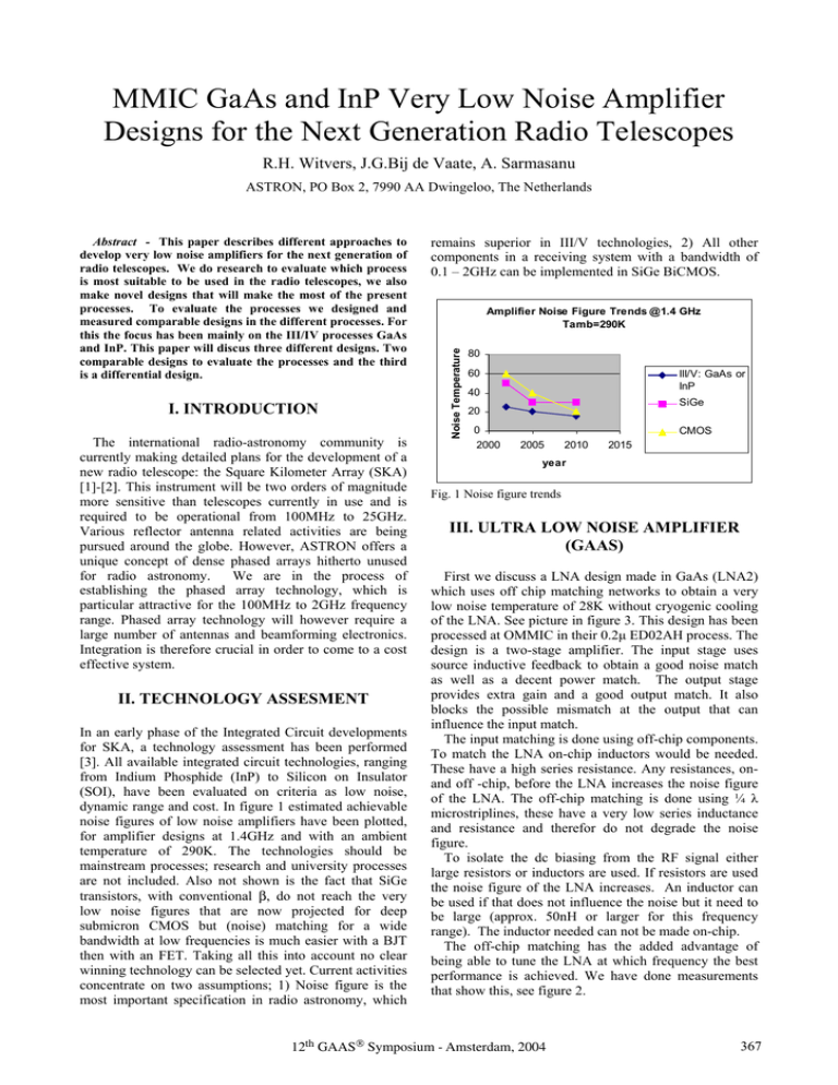
MMIC GaAs and InP Very Low Noise Amplifier Designs for the Next Generation Radio Telescopes R.H. Witvers, J.G.Bij de Vaate, A. Sarmasanu ASTRON, PO Box 2, 7990 AA Dwingeloo, The Netherlands I. INTRODUCTION The international radio-astronomy community is currently making detailed plans for the development of a new radio telescope: the Square Kilometer Array (SKA) [1]-[2]. This instrument will be two orders of magnitude more sensitive than telescopes currently in use and is required to be operational from 100MHz to 25GHz. Various reflector antenna related activities are being pursued around the globe. However, ASTRON offers a unique concept of dense phased arrays hitherto unused for radio astronomy. We are in the process of establishing the phased array technology, which is particular attractive for the 100MHz to 2GHz frequency range. Phased array technology will however require a large number of antennas and beamforming electronics. Integration is therefore crucial in order to come to a cost effective system. II. TECHNOLOGY ASSESMENT In an early phase of the Integrated Circuit developments for SKA, a technology assessment has been performed [3]. All available integrated circuit technologies, ranging from Indium Phosphide (InP) to Silicon on Insulator (SOI), have been evaluated on criteria as low noise, dynamic range and cost. In figure 1 estimated achievable noise figures of low noise amplifiers have been plotted, for amplifier designs at 1.4GHz and with an ambient temperature of 290K. The technologies should be mainstream processes; research and university processes are not included. Also not shown is the fact that SiGe transistors, with conventional β, do not reach the very low noise figures that are now projected for deep submicron CMOS but (noise) matching for a wide bandwidth at low frequencies is much easier with a BJT then with an FET. Taking all this into account no clear winning technology can be selected yet. Current activities concentrate on two assumptions; 1) Noise figure is the most important specification in radio astronomy, which remains superior in III/V technologies, 2) All other components in a receiving system with a bandwidth of 0.1 – 2GHz can be implemented in SiGe BiCMOS. Amplifier Noise Figure Trends @1.4 GHz Tamb=290K Noise Temperature Abstract - This paper describes different approaches to develop very low noise amplifiers for the next generation of radio telescopes. We do research to evaluate which process is most suitable to be used in the radio telescopes, we also make novel designs that will make the most of the present processes. To evaluate the processes we designed and measured comparable designs in the different processes. For this the focus has been mainly on the III/IV processes GaAs and InP. This paper will discus three different designs. Two comparable designs to evaluate the processes and the third is a differential design. 80 60 III/V: GaAs or InP 40 SiGe 20 0 2000 CMOS 2005 2010 2015 year Fig. 1 Noise figure trends III. ULTRA LOW NOISE AMPLIFIER (GAAS) First we discuss a LNA design made in GaAs (LNA2) which uses off chip matching networks to obtain a very low noise temperature of 28K without cryogenic cooling of the LNA. See picture in figure 3. This design has been processed at OMMIC in their 0.2µ ED02AH process. The design is a two-stage amplifier. The input stage uses source inductive feedback to obtain a good noise match as well as a decent power match. The output stage provides extra gain and a good output match. It also blocks the possible mismatch at the output that can influence the input match. The input matching is done using off-chip components. To match the LNA on-chip inductors would be needed. These have a high series resistance. Any resistances, onand off -chip, before the LNA increases the noise figure of the LNA. The off-chip matching is done using ¼ Ȝ microstriplines, these have a very low series inductance and resistance and therefor do not degrade the noise figure. To isolate the dc biasing from the RF signal either large resistors or inductors are used. If resistors are used the noise figure of the LNA increases. An inductor can be used if that does not influence the noise but it need to be large (approx. 50nH or larger for this frequency range). The inductor needed can not be made on-chip. The off-chip matching has the added advantage of being able to tune the LNA at which frequency the best performance is achieved. We have done measurements that show this, see figure 2. 12th GAAS Symposium - Amsterdam, 2004 367 45 2 1,8 1,6 1,4 1,2 1 0,8 0,6 0,4 0,2 0 40 30 25 20 15 Gain [dB] 35 Measured Noise Simulated Noise Measured Gain Simulated Gain 10 5 1500 1400 1300 1200 1100 900 1000 800 700 600 0 500 Noise Figure [dB] Noise measurements LNA2 freq [MHz] Fig. 2 Noise measurements on GaAs LNA provide the amplifier with balanced signals. These circuits need to be characterized very accurately themselves. This gives no direct access to the input and output ports of the amplifier which complicates the characterization. A number of passive, micro-strip type circuits are available to be used to do the unbalanced to balanced conversion but they are all bandwidth limited. We have therefore divided the frequency band into narrower bands to do the measurements. The other approach taken is to directly connect the amplifier to the antenna and do without the unbalanced to balanced conversion. Details of the complete active antenna test issues can be found in [4]. Frequency [GHz] 1 2 3 4 5 Gain [dB] 23 24 23 22 20 Noise temperature [K] 46 40 38 38 44 Table 1 Fig. 3 Picture GaAs LNA IV. DIFFERENTIAL LNA (GAAS) The second design is a balanced LNA (DLNA7) to be used combined with a dipole type antenna. This design has been processed at OMMIC in their ED02AH process. Using the LNA as an active balun improves the noise performance of the active antenna considerably. This because losses between antenna and LNA will show up as noise and increase the noise temperature of the system. The LNA has been designed to work from 2.5 to 5 GHz. The input impedance chosen is 150 ȍ. The optimum noise impedance for these hemts is high and inductive and an higher input impedance reduces the circuitry needed for the match and therefore the losses before the amplifier. Also the antenna sees a higher impedance to the air. Choosing an higher input impedance for the amplifier reduces the impedance step that should be achieved by the antenna. A picture of the IC can be seen in Figure 4. The design consists of two differential stages, see figure 5. The first stage uses source inductive feedback for a good noise and power match. It has relatively large drain resistors that will give good gain and noise performance but decreases the intermodulation performance. The second stage is used to equalize the gain, using local feedback, and give a good output match and to improve the intermodulation performance. For the simulated s-par results see figure 6, see figure 7 for the noise temperature. Characterizing a balanced amplifier, in particular for large signal behavior and noise performance, is less straightforward then for an unbalanced design. Because most measurement equipment (vna’s and spectrum analysers) is unbalanced extra circuitry is needed to 368 Fig. 4 Picture of balanced LNA 5v 5v 50 110 2 .5 n H 120 6 x4 0 6 x6 0 6 x6 0 6 x4 0 2 .5 n H 120 110 5v 50 5v Fig. 5 Schematic of balanced LNA Fig. 6 Simulated S-par of balanced LNA 12th GAAS Symposium - Amsterdam, 2004 Fig. 7 Noise performance balanced LNA Fig. 8 Picture of the InP LNA V. WIDEBAND LOW NOISE AMPLIFIER (INP) The third design is an InP LNA design (LNA4), see figure 8. The IC is a 0.10 um process and has been processed at NG Velocium. InP has a better noise performance then GaAs but has the disadvantage being a process suitable for higher frequencies. It is harder to obtain a good noise and power match for InP then for GaAs at these relatively low frequencies. The LNA has all the circuitry to bias on-chip and can be used without any matching circuitry. The plots in figure 9 show the sparameter performance found in the simulator and figure 11 show the S21measured on a large number of ICs using a wafer prober. As can be seen the shape of the curves compares well only the measurements show a higher gain. Figure 10 shows the simulated noise performance. The noise temperature is below 40K from 2.8 to 4.6GHz. This is slightly higher then the GaAs design featured in the beginning of this paper but over a much larger bandwidth. To evaluate the InP process compared to the GaAs design a separate version without the input biascircuitry has been made as well, LNA-3. This design shows a much lower noise temperature, below 20K from 2.5 to 4.3GHz, because the matching components used can have much lower loss and therefore the LNA has a lower noise temperature. This shows a much better performance of InP over GaAs. But the use of InP has some practical drawbacks. The optimum input impedance for low noise performance is highly resistive and inductive. It is considerably more resistive then the GaAs process discussed before., for the lower frequencies. This makes the process less suitable to do this low frequency designs. For higher frequencies this process is preferred over GaAs. The process is far less accessible and more expensive then GaAs. This is an important point because cost will be a major driver for the next generations of telescopes where large number of devices is needed. Fig. 9 simulated s-par of LNA-4 Fig. 10 Simulated noise temperature LNA-4 Fig. 11 Measured S21 LNA-4 12th GAAS Symposium - Amsterdam, 2004 369 VI. CONCLUSION The results have been presented for Low Noise Amplifier MMIC designs at room temperature, based on standard III/V processes. Based on these results, it can be concluded that a high integration can indeed give high band-width and low noise temperatures, required for SKA REFERENCES [1] www.skatelescope.org [2] A. van Ardenne, A. B. Smolders and G. A. Hampson, “Active adaptive antennas for Radio Astronomy; results for the R&D program towards the Square Kilometre Array”, SPIE conference, Munich, Germany, March 2000 [3] J.G. Bij de Vaate, “RF-IC Developments for Wide Band Phased Array Systems”, Perspectives on Radio Astronomy: Technology for Large Antenna Arrays, Dwingeloo, The Netherlands, April 1999 [4] J.G. Bij de Vaate, D. Geskus, R.H. Witvers, Integrated Active Antenna noise Figure Characterization Using a Cryogenic Anechoic Noise Source, European Microwave Conference, London, UK, Sept 2001 370 12th GAAS Symposium - Amsterdam, 2004


