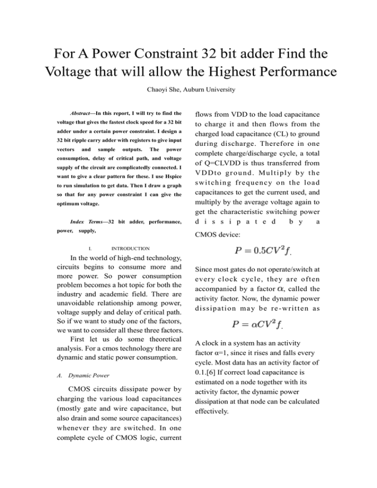
For A Power Constraint 32 bit adder Find the
Voltage that will allow the Highest Performance
Chaoyi She, Auburn University
Abstract—In this report, I will try to find the
voltage that gives the fastest clock speed for a 32 bit
adder under a certain power constraint. I design a
32 bit ripple carry adder with registers to give input
vectors
and
sample
outputs.
The
power
consumption, delay of critical path, and voltage
supply of the circuit are complicatedly connected. I
want to give a clear pattern for these. I use Hspice
to run simulation to get data. Then I draw a graph
so that for any power constraint I can give the
optimum voltage.
Index Terms—32 bit adder, performance,
power,
supply,
I.
flows from VDD to the load capacitance
to charge it and then flows from the
charged load capacitance (CL) to ground
during discharge. Therefore in one
complete charge/discharge cycle, a total
of Q=CLVDD is thus transferred from
VDDto ground. Multiply by the
swi t chi n g fr e qu e n c y o n t h e l oa d
capacitances to get the current used, and
multiply by the average voltage again to
get the characteristic switching power
d i s s i p a t e d
b y
a
CMOS device:
INTRODUCTION
In the world of high-end technology,
circuits begins to consume more and
more power. So power consumption
problem becomes a hot topic for both the
industry and academic field. There are
unavoidable relationship among power,
voltage supply and delay of critical path.
So if we want to study one of the factors,
we want to consider all these three factors.
First let us do some theoretical
analysis. For a cmos technology there are
dynamic and static power consumption.
A. Dynamic Power
CMOS circuits dissipate power by
charging the various load capacitances
(mostly gate and wire capacitance, but
also drain and some source capacitances)
whenever they are switched. In one
complete cycle of CMOS logic, current
.
Since most gates do not operate/switch at
ever y clock c ycl e, t he y are oft en
accompanied by a factor , called the
activity factor. Now, the dynamic power
di ssi p at i on m a y b e re - wri t t e n as
.
A clock in a system has an activity
factor α=1, since it rises and falls every
cycle. Most data has an activity factor of
0.1.[6] If correct load capacitance is
estimated on a node together with its
activity factor, the dynamic power
dissipation at that node can be calculated
effectively.
Since there is a finite rise/fall time
for both pMOS and nMOS, during
transition, for example, from off to on,
both the transistors will be on for a small
period of time in which current will find
a path directly from VDD to ground,
hence creating a short-circuit current.
Short-circuit power dissipation increases
with rise and fall time of the transistors.
A n a d di t i o na l fo r m o f p o w e r
consumption became significant in the
1990s as wires on chip became narrower
and the long wires became more resistive.
CMOS gates at the end of those resistive
wires see slow input transitions. During
the middle of these transitions, both the
NMOS and PMOS logic networks are
partially conductive, and current flows
directly from VDD to VSS. The power
thus used is called crowbar power.
Careful design which avoids weakly
driven long skinny wires ameliorates this
effect, but crowbar power can be a
substantial part of dynamic CMOS power.
To speed up designs, manufacturers
have switched to constructions that have
lower voltage thresholds but because of
this a modern NMOS transistor with a
Vth of
200 mV
has
a
significant subthreshold leakage current.
Designs (e.g. desktop processors) which
include vast numbers of circuits which
are not actively switching still consume
power because of this leakage current.
Leakage power is a significant portion of
the total power consumed by such
designs. Multi-threshold
CMOS (MTCMOS), now available from
foundries, is one approach to managing
leakage power. With MTCMOS, high
Vth transistors are used when switching
speed is very important, while low
Vth transistors are used in speed sensitive
paths. Further technology advances that
use even thinner gate dielectrics have an
additional leakage component because of
current tunnelling through the extremely
thin gate dielectric. Using high-k
dielectrics instead of silicon dioxide that
is the conventional gate dielectric allows
similar device performance, but with a
thicker gate insulator, thus avoiding this
current. Leakage power reduction using
new material and system designs is
critical to sustaining scaling of CMOS.
B. Static Power
Both NMOS and PMOS transistors
have a gate–source threshold voltage,
below which the current (called sub
threshold current) through the device
drops exponentially. Historically, CMOS
designs operated at supply voltages much
larger than their threshold voltages
(Vdd might have been 5 V, and Vth for
both NMOS and PMOS might have been
700 mV). A special type of the CMOS
transistor with near zero threshold
voltage is the native transistor.
II.
DESIGN
The design is a 32 bit ripple carry
adder. A full adder adds binary numbers
and accounts for values carried in as well
as out. A one-bit full adder adds three
one-bit numbers, often written as A, B,
and Cin; A and B are the operands,
and Cin is a bit carried in from the
previous less significant stage. I use 32 1
bit full adder to form a 32 bit ripple carry
adder. Each carry bit "ripples" to the next
full adder.
For giving clocks to the circuit, I add
registers before and after the input and
output of the adder.
The technology I use is 45 nm low
power technology.
III.
SIMULATION
Minumun
power(w)
6.80E-03
1.76
1.7
8.18E-03
1.66
1.8
9.51E-03d
1.58
Table 1. voltage, power and min clock cycle
I use Hspice to make the simulation.
I assume that here “best performance”
means fastest speed. I will first specify
some voltage and under that voltage I use
some tests to find the fastest clock and
then find power consumption under this
condition.
But the question is that is this voltage
the best one under this power, or is there
any other voltage could give me faster
clock but less power?
The answer is no. If there really
exists such a voltage, and if it is higher
than the current voltage we have found,
the faster clock and higher voltage will
not satisfy power constraint. And if that
another voltage is lower than the voltage
we have found, it will not give me faster
clock.
Here is the complete data table.
voltage(v)
1.6
clock
cycle(ns)
0.7
3.52E-04
17.8
0.8
6.84E-04
8.2
0.9
9.92E-04
5.14
1
1.46E-03
3.78
1.1
2.07E-03
3.04
1.2
2.89E-03
2.6
1.3
3.41E-03
2.28
1.4
4.63E-03
2.06
1.5
5.73E-03
1.92
From this table, we can see that as
the voltage increase, power consumption
increase and minimum clock cycle drops.
So here is the diagram for power and
voltage relationship.
Figure 1. Power and voltage
From this graph, we can see that
power increases as voltage increases. So
if our customer requires some power
constraint, we can draw a horizontal line
with that power value, then draw a
vertical line at the crossing point. The
voltage at the vertical line is the most
optimum voltage under that power
constraint. In a word, I can give all the
best voltage that allow highest
performance if the power constraint is
given in the range of Table 1.
IV.
Conclusions and expectations
From this project, I get a clear
pattern of power, delay and voltage
supply relationship. With these data, I can
do more work. If I can get critical path
delay, I can calculate the power-delay
product, so I can set the most optimum
voltage for this circuit. What is more,
with alpha-power law, I can even
estimate what value of alpha is. These are
what I am going to do in future.
References
[1] Baker, R. Jacob (2008). CMOS: circuit design, layout, and
simulation(Second ed.). Wiley-IEEE. p. xxix. ISBN 978-0470-22941-5.
[2] A good overview of leakage and reduction methods are
explained in the book Leakage in Nanometer CMOS
Technologies ISBN 0-387-25737-3.
[3] Weste, Neil H. E. and Harris, David M. (2010). CMOS
VLSI Design: A Circuits and Systems Perspective, Fourth
Edition. Boston: Pearson/Addison-Wesley. p. 840. ISBN 9780-321-54774-3.
[4] M. Morris Mano, Digital Logic and Computer Design,
Prentice-Hall 1979, 0-13-214510-3 pp.119-123


