Data transmission architecture
advertisement
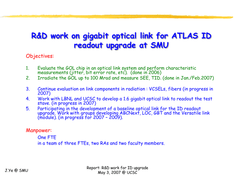
R&D work on gigabit optical link for ATLAS ID readout upgrade at SMU Objectives: 1. 2. 3. 4. 5. Evaluate the GOL chip in an optical link system and perform characteristic measurements (jitter, bit error rate, etc). (done in 2006) Irradiate the GOL up to 100 Mrad and measure SEE, TID. (done in Jan./Feb.2007) Continue evaluation on link components in radiation : VCSELs, fibers (in progress in 2007) Work with LBNL and UCSC to develop a 1.6 gigabit optical link to readout the test stave. (in progress in 2007) Participating in the development of a baseline optical link for the ID readout upgrade. Work with groups developing ABCNext, LOC, GBT and the Versatile link (module). (in progress for 2007 – 2009). Manpower: One FTE in a team of three FTEs, two RAs and two faculty members. J.Ye @ SMU Report: R&D work for ID upgrade May 3, 2007 @ UCSC Test results on the GOL in 2006 – 2007 1. (1) The test system designed and constructed for in-lab and irradiation tests: 32 bits/40 MHz 16 bits/80 MHz A big board for a small chip: For in-lab (BER, jitter and powerup schemes) and irradiation (gamma, proton and neutron) tests. The upper 3U crate hosts boards in the beam (gamma or proton). The VCSEL is mounted 2 mm away from the GOL. The LC connector is 4×4 mm2 cross, and 50 mm boot length. The fiber is 1.6 mm OD. The lower 6U crate hosts controlling and DAQ boards. The master PC can be placed 40 meters away, connecting with USB. GOL: 13×13mm2×1.7mm, ~400 mW. LabVIEW based GUI. J.Ye @ SMU Report: R&D work for ID upgrade May 3, 2007 @ UCSC The actual PCB space needed for in the actual application will be less than 20 mm × 30 mm (the red mark). Test results on the GOL in 2006 – 2007 (2) 2. In-lab characterization tests on the GOL: o Bit Error Rate (BER): o o Power-up schemes studied and found to be reliable. The jitter tests: • • Tr-225ps, Tf-245ps. Eye mask test. • GOL reference clock jitter transfer function: Clock jitter cutoff at about 1 MHz. Complies with the adapted IEEE standards. Low frequency jitter (noise) source at the system level needs to be watched for. • J.Ye @ SMU GOL-TLK optical link jitter tolerance: Jitter tolerance complies with the IEEE standard. This plot specifies the transmitter reference clock jitter to be below the blue line to achieve a BER less than 10-12. Report: R&D work for ID upgrade May 3, 2007 @ UCSC BER > 10-12 BER < 10-12 Test results on the GOL in 2006 – 2007 3. (3) Irradiation tests on GOL: o o o Source: 230 MeV proton. Tests: TID up to 106 Mrad (Si); SEE cross section (probability). Results: TID: • No supply current increase during the irradiation. GOL functions error free immediately after the beam is off, very small change in eye diagram and jitter. survives the TID test of 106 Mrad(Si) Before irradiation Eye diagram: before (left) and after After irradiation Jitter Components Tx clk Serial Data Tx clk Serial Data Random (RMS) 10.2ps 4.6ps 11.1ps 4.7ps Deterministic (Pk-Pk) 67.6ps 55.6ps 67.0ps 57.9ps Total@BER-14 196.1ps 106.7ps 211.7ps 111.8ps SEE: very small SEE cross section. Fluence (protons/cm2) Dose (Mrad(Si)) < 6 x 10⁸ 1 x 10¹¹ 5 x 10⁻³ 0 0 < 2.7 x 10⁻¹¹ < 2.7 x 10⁻¹¹ 1 x 10⁹ 3.7 x 10¹² 0.2 1 0 2.7 x 10⁻¹³ <2.7 x 10⁻¹³ 2 x 10¹⁰ 7.6 x 10¹³ 4 17 4 2.2 x 10⁻¹³ 5.3 x 10⁻¹⁴ 5 x 10¹¹ 1.9 x 10¹⁵ 100 200 20 1.1 x 10⁻¹³ 1.1 x 10⁻¹⁴ J.Ye @ SMU SEU events LoL Bit Error Cross-section (cm2) LoL Bit Error Flux (protons/cm2/s) Report: R&D work for ID upgrade May 3, 2007 @ UCSC Test results on VCSEL and fiber in 2006 – 2007 4. Tests on fiber and VCSEL. The Fiber: o Infinicor SX+ 50/250m/1.6mm MM 10G fiber from Corning. Germanium doped. o Tested wit Gamma (Co-60) and Proton (230 MeV, 1.9×10¹³ proton/cm2). o Very small light loss at low flux (dose rate). Big loss at high flux but anneals very quickly (within 1 hour) back. o Very promising for LHC upgrade. o More tests with gamma needed. The VCSEL: o Two HFE6192-562 (10G LC w/ 50 ohm flex) from Finisar tested . o Irradiated with 230 MeV proton, 1.9×10¹³ proton/cm2. o The VCSELs are biased during irradiations. o Eye diagram – see plots and table. o Looks very promising but more tests needed. Before irradiation After irradiation Rise/fall time (ps) O-power (W) Rise/fall time (ps) O-power (W) L1 114/130 431 110/128 133 L2 120/132 450 122/132 295 VCSEL J.Ye @ SMU Report: R&D work for ID upgrade May 3, 2007 @ UCSC L1, before irradiation L1, after irradiation Conclusions on the GOL, VCSEL and fiber evaluation 1. GOL complies with the adapted (to 1.6 Gbps) IEEE standard for Gigabit Ethernet (1.25 Gbps). 2. GOL is tested to be rad-resistant up to 106 Mrad (Si). 3. The SEE probability is measured to be 1.1×10⁻¹³ for link frame loss and 1.1×10⁻¹⁴ for single bit flip. The GOL chip is a good candidate for 1.6 Gbps optical link, radhard to the ID requirement. 4. We have preliminary candidates for the VCSEL and the fiber. J.Ye @ SMU Report: R&D work for ID upgrade May 3, 2007 @ UCSC Plans for 2007 and 2008 1. Issues on a gigabit optical link architecture: 2. To address the above issues, we plan to: o o o o o Rad-hard serializer + TOSA (driver, VCSEL), Rad-hard fiber, Reference clock jitter control (cleaning), Input data bit-to-bit skew control, Reliability and single point failure prevention. o Collaborate with LBNL and UCSC to construct a GOL based prototype link to readout the test stave. • To study gigabit link system issues with the ABCNext (ABCD for now) upstream electronics, with the QPLL clock jitter cleaner. • A dual link system will be investigated to address The single point failure, The SEE o o o J.Ye @ SMU • CERN QPLL chip will be used as the clock cleaner. Do more irradiation tests on fiber and VCSEL to identify candidates for a multi-gigabit optical link for SLHC ID readout upgrade. Carry out reliability tests on the GOL, TOSA to provide info about the redundancy in the link. Investigate the LOC and the GBT as the serializer chip when they become available for higher bandwidth link. Report: R&D work for ID upgrade May 3, 2007 @ UCSC clock Delay lines connector data (32) LVDS CMOS Our design of the GOL based prototype optical link (1) Delay line + QPLL fiber TOSA GOL fiber VCSEL Control logic The transmitter board. The output can be chosen to go through TOSA (CERN rad-hard versatile link) or a VCSEL to avoid failures in the optical device and fiber. The delay line in the data bus is used to address the bit-to-bit skew problem. In ABCnext, this delay will be implememented. J.Ye @ SMU Report: R&D work for ID upgrade May 3, 2007 @ UCSC PIN+TIA+LA TLK 2500 The receiver board J.Ye @ SMU Report: R&D work for ID upgrade May 3, 2007 @ UCSC connector ROSA CMOS LVDS fiber 1:2 deMUX Our design of the GOL based prototype optical link (2) data (32) clock Budget (for 2008) manpower One FTE @ $55k/yr, w/ 25% benefit $68.75k M&S PCB fab. + assembly + components $10k Travel For gamma irradiation tests only $5k Others Reliability test $0 Total With SMU 45.5% overhead $121.85k J.Ye @ SMU Report: R&D work for ID upgrade May 3, 2007 @ UCSC
