ix TABLE OF CONTENTS CHAPTER
advertisement
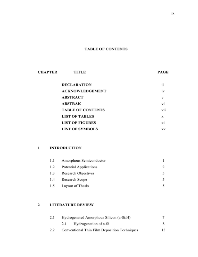
ix TABLE OF CONTENTS CHAPTER 1 2 TITLE PAGE DECLARATION ii ACKNOWLEDGEMENT iv ABSTRACT v ABSTRAK vi TABLE OF CONTENTS vii LIST OF TABLES x LIST OF FIGURES xi LIST OF SYMBOLS xv INTRODUCTION 1.1 Amorphous Semiconductor 1 1.2 Potential Applications 2 1.3 Research Objectives 5 1.4 Research Scope 5 1.5 Layout of Thesis 5 LITERATURE REVIEW 2.1 2.2 Hydrogenated Amorphous Silicon (a-Si:H) 7 2.1 8 Hydrogenation of a-Si Conventional Thin Film Deposition Techniques 13 x 2.2.1 Chemical Vapor Deposition 13 2.2.2 DC Glow Discharge 14 2.2.3 RF Glow Discharge 18 2.3 Plasma Enhanced Chemical Vapor Deposition (PECVD) 19 2.4 Plasma Fundamentals 19 2.4.1 19 2.5 3 Non-equilibrium Glow Discharges 2.4.2 Potentials in rf Glow Discharges 21 Qualitative Model for PECVD Reactions 22 METHODOLOGY 3.1 3.2 Deposition of Amorphous Silicon Films 27 3.1.1 Introduction 27 3.1.2 27 Plasma Enhanced Chemical Vapor Deposition 3.1.3 PECVD Setup 28 3.1.4 PECVD System Deposition Process 33 3.1.5 Preparation of a-Si:H Samples 34 3.1.5.1 Substrate Preparation 34 3.1.5.2 34 Deposition Parameters Analytical Tools 36 3.2.1 36 Spectroscopy 3.2.2 Absorption 3.2.3 37 3.2.2.1 Optical Absorption 37 3.2.2.2 42 UV-3101-PC Spectrophotometer Infrared (IR) Absorption Spectroscopy 45 3.2.3.1 Introduction 45 3.2.3.2 45 Mechanism of IR Absorption 3.2.3.3 FTIR – Fourier Transform Infrared Spectroscopy 3.2.4 3.2.5 46 Photoluminescence 49 3.2.4.1 Basic Theory of Photoluminescence 49 3.2.4.2 Luminescence Spectrometer LS 55 51 Atomic Force Microscopy (AFM) 54 xi 3.2.5.1 Contact Mode 3.2.5.2 Non-contact Mode 57 3.2.5.3 Tapping Mode 57 3.2.5.4 Image Display 57 3.2.5.5 Surface Roughness 3.3 4 5 56 Film Thickness Measurements 58 58 RESULTS AND DISCUSSIONS 4.1 Surface Morphology and Deposition Rate 61 4.2 X-Ray Diffraction (XRD) Analysis 70 4.3 Infrared (IR) Transmission Spectrum 72 4.3.1 Dependence on rf Power 74 4.3.2 79 Dependence on Substrate Temperature 4.4 Optical Energy Gap 84 4.5 Photoluminescence 89 4.5.1 89 Dependence on Substrate Temperature CONCLUSION 5.1 Summary 96 5.2 Recommendation 98 REFERENCES 99 PRESENTATIONS 105 xii LIST OF TABLE TABLE NO. 3.1 TITLE PAGE The preparation conditions for a-Si:H thin films under different RF power and substrate temperature. Note that 4.1 other parameters are kept constant. 35 The observed mode frequency and their assignments. 72 xiii LIST OF FIGURES FIGURE NO. 1.1 TITLE PAGE Schematic representation of a typical thin film a-Si:H solar cell on glass. The incoming photons with an energy larger than the band gap are absorbed in the intrinsic a-Si:H film creating holes-electron pairs. 3 1.2 Schematic of a general active matrix array. 4 2.1 A model of hydrogenated amorphous silicon. The small ball represent hydrogen atoms while the large ball represents silicon atoms. 2.2 Model for the adsorption, diffusion and recombination of SiH3 on the growing surface. 2.3 9 12 A common implementation of CVD (AX, X, BX – gases, AB – solid material). 14 2.4 Current-voltage characteristics in a DC glow discharge. 15 2.5 Luminous zones and dark spaces in a DC glow discharges. 2.6 The potential distribution in a DC glow discharge. (Vp – plasma potential, Vc – cathode potential). 2.7 17 Schematic of fundamental transport and reaction processes underlying CVD. 2.8 16 23 Equivalent circuit representation of the sequence of steps in thermally driven CVD. The Ri (with i = 1-7) represent the seven steps describe in the text. 2.9 Equivalent circuit representation showing the thermal CVD path, and the parallel plasma-enhanced path 24 xiv represented by the Ri*s. 2.10 25 Activation energy diagram for a thermally driven (solid line) and plasma enhanced (dashed line) reaction. The activation energy for the plasma enhanced reaction, ∆E*, is typically less than that for the thermally driven reaction, ∆E. 26 3.1 NPN2 gas. 29 3.2 PN2 gas rack. 29 3.3 Silane (SiH4) gas cabinet. 30 3.4 Scrubber. 30 3.5 Schematic of the rf PECVD reactor system. 31 3.6 The rf PECVD reactor system. 32 3.7 A schematic of the optical absorption curves of amorphous materials. 3.8 39 Electron transition for semiconductors having a direct gap and indirect gap 40 3.9 Shimadzu UV-3101-PC Spectrophotometer. 44 3.10 Examples of infrared active and inactive absorption bands in CO2. 3.11 46 Fourier transform infrared spectrometer (Perkin Elmer Spectrum GX). 48 3.12 A schematic of the PL process. 50 3.13 Photoluminescence spectrometer LS 55. 52 3.14 Luminescence spectrometer schematic diagram. 54 3.15 Beam deflection system, using a laser and photodetector to measure the beam position. 55 3.16 Force between tip and sample surface 56 3.17 Colour mapping scheme for height 58 3.18 Dektak3 surface profiler. 59 4.1 Representation of surface morphology of a-Si:H films. 63 4.2 The 10 µm × 10 µm AFM images with surface height given by the grey scales extending from 0 (black) to 400 nm (white): (a) sample A deposited at 27°C; (b) sample B deposited at 100°C; (c) sample C xv deposited at 200°C; (d) sample D deposited at 300°C. 4.3 Deposition rate of a-Si:H films deposited at different temperature as a function of rf power. 4.4 69 X-ray diffraction pattern of a-Si:H thin film deposited at room temperature and rf power of 100 W. 4.7 68 Model of surface reaction where Si-Si is formed releasing H2. 4.6 67 Deposition rate of a-Si:H films deposited at different rf power as a function of substrate temperature. 4.5 64 70 X-ray diffraction pattern of a-Si:H thin film deposited at 200˚C and rf power of 50 W. 71 4.8 Local Si-H vibrations for SiH, SiH2 and SiH3 groups. 72 4.9 IR transmission of a-Si:H thin films deposited at different rf power. Emphasize on the 2000 cm-1 regime. 4.10 IR transmission of a-Si:H thin films deposited at different rf power. Emphasize on the 600 cm-1 regime. 4.11 77 IR transmission of a-Si:H thin film prepared under different rf power by Lucovsky et al. (1979) 4.13 76 IR transmission of a-Si:H thin films deposited at different rf power. Emphasize on the 800 cm-1 regime. 4.12 75 78 IR transmission of a-Si:H thin films deposited at different substrate temperatures. Emphasize on the 2000 cm-1 regime. RF power is at 100 W. 4.14 81 IR transmission of a-Si:H thin films deposited at different substrate temperatures. Emphasize on the 800 cm-1 regime. RF power is at 100 W. 4.15 82 IR transmission of a-Si:H thin films deposited at different substrate temperatures. Emphasize on the 600 cm-1 regime. RF power is at 100 W. 4.16 The (αhν)1/2 vs hν graphs for a-Si:H deposited at different rf power. 4.17 84 The (αhν)1/2 vs hν graphs for a-Si:H deposited at different substrate temperature. 4.18 83 Energy gap of a-Si:H films prepared under different 85 xvi substrates temperatures as a function of rf power. 4.19 86 Luminescence spectrum of amorphous silicon at various substrate temperatures with rf power kept constant at 50W. 4.20 90 Luminescence spectrum of amorphous silicon at various substrate temperatures with rf power kept constant at 100W. 4.21 91 Luminescence spectrum of amorphous silicon at various substrate temperatures with rf power kept constant at 150W. 4.22 91 Luminescence spectrum of amorphous silicon at various substrate temperatures with rf power kept constant at 200W. 4.23 92 Luminescence spectrum of amorphous silicon at various substrate temperatures with rf power kept constant at 250W. 4.24 92 Flow diagram representing the interrelation of the excitation and recombination processes appropriate to amorphous silicon. 4.25 94 Schematic plot of the relaxation and recombination probabilities versus energy from midgap. 95 xvii LIST OF SYMBOL VB - Breakdown voltage VG - Glow discharge voltage Vp - Plasma potential Vc - Cathode potential Vf - Floating potential A - Gas species A* - Reactive species e- - Electrons e - Unit electron charge (1.60 × 10⁻¹⁹ C) k1 - Reaction rate coefficient Te - Electron temperature Ts - Substrate temperature mi - Ion mass me - Electron mass k - Boltzmann constant (1.38 × 10⁻²³ J/K) ∆E* - Activation energy for plasma enhanced reaction ∆E - Thermally driven activation energy Eg - Optical gap Eo - Urbach energy α - Optical absorption h - Planck constant (6.625 × 10⁻³⁴ J-s) ν - Frequency B - Edge width parameter A - Absorbance T - Transmittance Io - Incident light intensity xviii I - Intensity of light transmitted through sample d - Film thickness t - Deposition time c - Speed of light (2.998 × 10⁸ m/s) λ - Wavelength of light Ds - Surface diffusion τs - Staying time dr - Deposition rate CH - Bonded H content XC - Volume fraction of microcrystalline
