SDRAM Controller Megafunction
Solution Brief 38
Target Applications:
Embedded systems for
telecommunications, networking,
graphics, and industrial controls
Family:
FLEX® 10K
April 1999, ver. 1
Features
■
■
■
■
■
■
Fully synchronous design
All signals are registered on the rising edge of the system clock
Simple request/acknowledge interface to the application
Standard interface to the SDRAM, compatible with typical SDRAMs
Tracks SDRAM refreshes
Includes option to power down the SDRAM for low-power applications
Vendor:
General Description
Stargate Solutions, Inc.
2355 Old Oakland Road, Suite 33
San Jose, CA 95131
Info@sgates.com
http://www.sgates.com
The SDRAM controller megafunction provides a simple request/handshake interface to
the application and a standard interface to the SDRAM. The megafunction handles all
SDRAM-related command generation and data transfers, including refresh generation.
Thus, the megafunction hides all protocol-related complexities from the application.
Functional Description
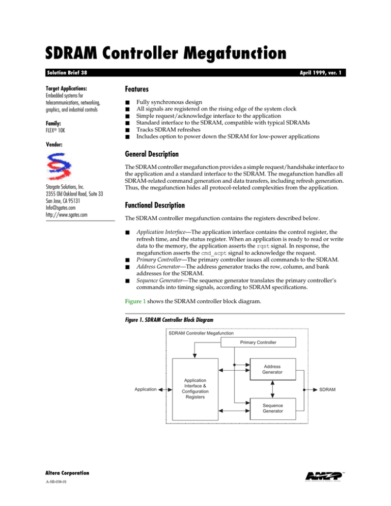
The SDRAM controller megafunction contains the registers described below.
■
■
■
■
Application Interface—The application interface contains the control register, the
refresh time, and the status register. When an application is ready to read or write
data to the memory, the application asserts the rqst signal. In response, the
megafunction asserts the cmd_acpt signal to acknowledge the request.
Primary Controller—The primary controller issues all commands to the SDRAM.
Address Generator—The address generator tracks the row, column, and bank
addresses for the SDRAM.
Sequence Generator—The sequence generator translates the primary controller’s
commands into timing signals, according to SDRAM specifications.
Figure 1 shows the SDRAM controller block diagram.
Figure 1. SDRAM Controller Block Diagram
SDRAM Controller Megafunction
Primary Controller
Address
Generator
Application
Application
Interface &
Configuration
Registers
SDRAM
Sequence
Generator
Altera Corporation
A-SB-038-01
SM
ALTERA MEGAFUNCTION PARTNERS PROGRAM
ALTERA MEGAFUNCTION PARTNERS PROGRAM
SB 38: SDRAM Controller Megafunction
Ports
Tables 1 and 2 show the megafunction’s input and output ports used by the application.
Table 1. Signals from the Application
Signal
Description
addr[21..0]
Address to the SDRAM. Provides the SDRAM row address, column address, and bank select. The address
is valid when rqst is asserted.
we_n
When low, data is written into memory. When high, data is read from memory. This signal is valid when
rqst is asserted.
wr_data[35..0]
Data written to the SDRAM. Contains 4 bytes of valid data and 4 parity bits.
rqst
Asserted when the application needs to access the memory. The addr[21..0], we_n, and
xfr_cnt[7..0] signals are valid when rqst is asserted. If we_n is low, the wr_data[35..0] bus is
also valid and it is the first valid data word of the transfer. The rqst signal is de-asserted when cmd_accpt
is sampled high by the application.
clk
System clock.
reset_n
Asynchronous active-low system reset. When reset, the controller goes idle. After reset, the controller waits
for the application to write to configuration register 0 and then initializes the SDRAM. The application should
wait for init_done to be asserted before issuing any commands to the controller.
cfg_wr[1..0]
Write enables for two configuration registers (i.e., configuration register 1 and configuration register 0). The
cfg_wr_data[31..0] bus is written into one of the two configuration registers when the corresponding
write enable bit is asserted in cfg_wr[1..0].
cfg_wr_data[31..0] Data written to one of the configuration registers.
cfg_rd[2..0]
Read enables for the three internal registers (i.e., configuration register 2, configuration register 1, and
configuration register 0). Data from one of the registers is placed on the cfg_rd_data[31..0] bus when
the corresponding bit is asserted in cfg_rd[2..0].
byte_en[3..0]
Indicates which of the four bytes in a data word are valid during a write operation. For a byte to be valid,
the corresponding bit in byte_en[3..0] should be high.
xfr_cnt[7..0]
Number of data words to be read or written to the SDRAM.
Table 2. Signals to the Application
Signal
Description
init_done
Level signal. Asserted high when the controller has finished initializing the SDRAM. The application should
wait for init_done to be asserted before requesting memory accesses. The init_done signal is deasserted when a reset occurs.
cmd_acpt
Asserted high for one-clock cycles to acknowledge the application’s rqst signal. The application should
de-assert rqst when cmd_acpt is sampled high.
nxt_dt_rqst
Active-high signal. Asserted to indicate that the controller has consumed the last piece of write data, and
the next write is requested from the application. When the application samples this signal high, it should
place the next data word on the wr_data[35..0] bus. If it is sampled low, the application should keep
the current data on wr_data[35..0].
nxt_dt_av
Active high level signal. When the application samples this signal high during a read transfer, the present
data on the rd_data[35..0] bus is valid. If the application samples this signal low, rd_data[35..0]
is not valid and the application should discard it.
rd_data[35..0]
Data read from the SDRAM. Valid when nxt_dt_av is asserted.
cfg_rd_data[31..0] Data read from the configuration registers.
lst_wr_xfr
Asserted high for one clock cycle to indicate that the current data word on wr_data[35..0] is the last
data word of the write transfer.
lst_rd_xfr
Asserted high for one clock cycle to indicate that the current data word on rd_data[35..0] is the last
data word of the read transfer.
2
Altera Corporation
SB 38: SDRAM Controller Megafunction
Table 3 shows the megafunction’s input and output ports used by the SDRAM.
Table 3. Signals to & from the SDRAM
Signal
Note
op_cke
Clock enable signal.
op_cs_n
This signal, along with the op_ras_n, op_cas_n, and op_we_n signals, defines the command issued
by the controller to the SDRAM.
op_ras_n
This signal, along with the op_cs_n, op_cas_n, and op_we_n signals, defines the command issued
by the controller to the SDRAM.
op_cas_n
This signal, along with the op_ras_n, op_cs_n, and op_we_n signals, defines the command issued
by the controller to the SDRAM.
op_we_n
This signal, along with the op_ras_n, op_cas_n, and op_cs_n signals, defines the command issued
by the controller to the SDRAM.
op_dqm[3..0]
Used as byte enables for the data to be written into the SDRAM. If any of the signal’s bits are high, the
corresponding byte on the SDRAM data bus will be masked.
op_bs[1..0]
SDRAM bank select.
op_ma[11..0]
SDRAM address.
op_md_oen_n
Active-low output enable signal for the bidirectional pads.
bp_md_i[35..0]
Data read from the SDRAM.
bp_md_o[35..0]
Data written to the SDRAM.
op_clk
Clock to the SDRAM. The SDRAM uses the internal design clock to gain access time.
Configuration Registers
The application must program the megafunction’s three configuration registers according to
the system’s requirements.
Configuration Register 0
Table 4 shows the format for configuration register 0. On reset, the megafunction waits for a
write to this register, and then initializes the SDRAM.
Table 4. Configuration Register 0 Format
Bits
Mnemonic
Description
0
num_ref
When set high, the primary controller performs 8 refreshes during
initialization. When set low, the primary controller performs 2
refreshes during initialization.
1
power_down
When set high, the primary controller places the SDRAM in powerdown mode. When reset low, the SDRAM exits power-down mode.
Configuration Register 1
Table 5 shows the format for configuration register 1.
Table 5. Configuration Register 1 Format
Altera Corporation
Bits
Mnemonic
Description
31..0
period64ms
Value of the 64-ms period, calculated using a clock whose period is
twice the input clock.
3
SB 38: SDRAM Controller Megafunction
Configuration Register 2
Table 6 shows the format for configuration register 2.
Table 6. Configuration Register 2 Format
Bit
Mnemonic
Description
0
ref_err
This bit is set when the primary controller cannot issue 4,096 refreshes
within a 64-ms period. It is reset when the application reads this
register.
31..1
reserved
Read back as 0s.
Performance
Table 7 describes the megafunction’s logic cell requirements for FLEX 10K devices.
Table 7. SDRAM Controller Megafunction Logic Cell Requirements
Device Family
Smallest Target
Device
Speed
Grade
FLEX 10K
EPF10K100E
-1
Note (1)
Device Utilization
Logic Cells
EABs
433
0
fMAX (MHz)
Availability
66
Now
Note:
(1)
Specifications are subject to change.
Deliverables
The SDRAM controller megafunction includes the following items:
■
■
■
■
■
OpenCoreTM evaluation
Documentation
Synthesis constraints
Simulation vectors
Register transfer level (RTL) code, as needed
®
101 Innovation Drive
San Jose, CA 95134
(408) 544-7000
http://www.altera.com
Copyright 1999 Altera Corporation. Altera, FLEX, FLEX 10K, EPF10K100E, OpenCore, and AMPP are trademarks and/or service marks
of Altera Corporation in the United States and other countries. Other brands or products are trademarks of their respective holders. The
specifications contained herein are subject to change without notice. Altera assumes no responsibility or liability arising out of the
application or use of any information, product, or service described herein except as expressly agreed to in writing by Altera Corporation.
Altera customers are advised to obtain the latest version of device specifications before relying on any published information and before
placing orders for products or services. All rights reserved.
Altera Corporation
4
