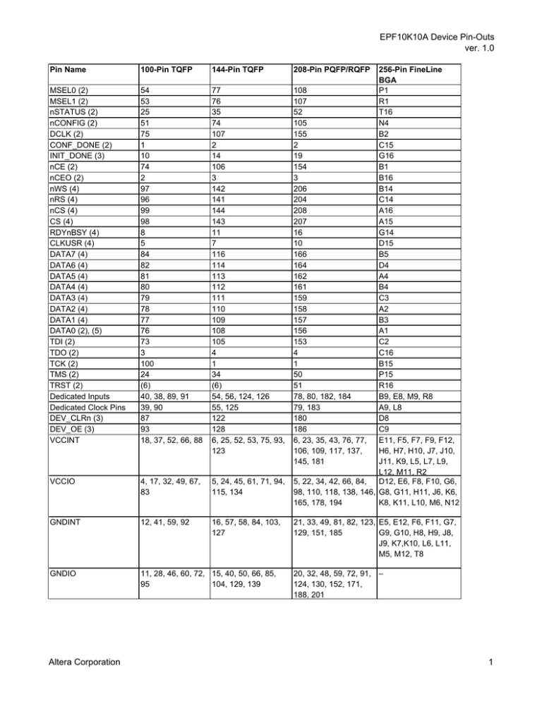
EPF10K10A Device Pin-Outs
ver. 1.0
Pin Name
100-Pin TQFP
144-Pin TQFP
MSEL0 (2)
MSEL1 (2)
nSTATUS (2)
nCONFIG (2)
DCLK (2)
CONF_DONE (2)
INIT_DONE (3)
nCE (2)
nCEO (2)
nWS (4)
nRS (4)
nCS (4)
CS (4)
RDYnBSY (4)
CLKUSR (4)
DATA7 (4)
DATA6 (4)
DATA5 (4)
DATA4 (4)
DATA3 (4)
DATA2 (4)
DATA1 (4)
DATA0 (2), (5)
TDI (2)
TDO (2)
TCK (2)
TMS (2)
TRST (2)
Dedicated Inputs
Dedicated Clock Pins
DEV_CLRn (3)
DEV_OE (3)
VCCINT
54
53
25
51
75
1
10
74
2
97
96
99
98
8
5
84
82
81
80
79
78
77
76
73
3
100
24
(6)
40, 38, 89, 91
39, 90
87
93
18, 37, 52, 66, 88
77
76
35
74
107
2
14
106
3
142
141
144
143
11
7
116
114
113
112
111
110
109
108
105
4
1
34
(6)
54, 56, 124, 126
55, 125
122
128
6, 25, 52, 53, 75, 93,
123
VCCIO
4, 17, 32, 49, 67,
83
5, 24, 45, 61, 71, 94,
115, 134
GNDINT
12, 41, 59, 92
16, 57, 58, 84, 103,
127
GNDIO
11, 28, 46, 60, 72, 15, 40, 50, 66, 85,
95
104, 129, 139
Altera Corporation
208-Pin PQFP/RQFP
256-Pin FineLine
BGA
108
P1
107
R1
52
T16
105
N4
155
B2
2
C15
19
G16
154
B1
3
B16
206
B14
204
C14
208
A16
207
A15
16
G14
10
D15
166
B5
164
D4
162
A4
161
B4
159
C3
158
A2
157
B3
156
A1
153
C2
4
C16
1
B15
50
P15
51
R16
78, 80, 182, 184
B9, E8, M9, R8
79, 183
A9, L8
180
D8
186
C9
E11, F5, F7, F9, F12,
6, 23, 35, 43, 76, 77,
H6, H7, H10, J7, J10,
106, 109, 117, 137,
J11, K9, L5, L7, L9,
145, 181
L12, M11, R2
D12, E6, F8, F10, G6,
5, 22, 34, 42, 66, 84,
98, 110, 118, 138, 146, G8, G11, H11, J6, K6,
K8, K11, L10, M6, N12
165, 178, 194
21, 33, 49, 81, 82, 123, E5, E12, F6, F11, G7,
129, 151, 185
G9, G10, H8, H9, J8,
J9, K7,K10, L6, L11,
M5, M12, T8
20, 32, 48, 59, 72, 91, –
124, 130, 152, 171,
188, 201
1
EPF10K10A Device Pin-Outs
ver. 1.0
Pin Name
100-Pin TQFP
144-Pin TQFP
No Connect (N.C.) (7)
–
–
Total User I/O Pins (8)
66
102
Altera Corporation
208-Pin PQFP/RQFP
256-Pin FineLine
BGA
7, 8, 9, 14, 15, 36, 37, A8, B8, D1, D14, D16,
E1, E3, E13, E14,
113, 114, 125, 126,
E15, E16, F14, F15,
139, 140
F16, G3, H1, H4, H16,
J1, J2, K2, K3, K12,
K14, K15, K16, L2, L4,
M2, M3, M4, M14,
M16, N1, N2, N3, N14,
N15, P2, P11, P14 (7)
134
150
2
EPF10K10A Device Pin-Outs
ver. 1.0
Notes:
(1) All pins that are not listed are user I/O pins.
(2) This pin is a dedicated pin; it is not available as a user I/O pin.
(3) This pin can be used as a user I/O pin if it is not used for its device-wide or configuration
function.
(4) This pin can be used as a user I/O pin after configuration.
(5) This pin is tri-stated in user mode.
(6) The optional JTAG pin TRST is not used in the 100-pin or 144-pin TQFP package.
(7) To maintain pin compatibility when transferring to the EPF10K10 or EPF10K10A device from any
other device in the 208-pin PQFP or 256-pin FineLine BGA package, do not use these pins as
user I/O pins.
(8) The user I/O pin count includes dedicated input pins, dedicated clock pins, and all I/O pins.
(9) To maintain pin compatibility when transferring to the EPF10K30 device from any other device in
the 356-pin BGA or 484-pin FineLine BGA package, do not use these pins as user I/O pins.
(10) To maintain pin compatibility when transferring to the EPF10K50V device from any other device
in the 484-pin FineLine BGA package, do not use these pins as user I/O pins.
(11) To maintain pin compatibility when transferring from the EPF10K100 to the EPF10K70 in the 503pin PGA package, do not use these pins as user I/O pins.
(12) This pin shows the status of the ClockLock and ClockBoost circuitry. When the ClockLock and
ClockBoost circuitry are locked to the incoming clock and generate an internal clock, LOCK is
driven high. LOCK remains high if a periodic clock stops clocking. The LOCK function is optional;
if the LOCK output is not used, this pin is a user I/O pin.
(13) This pin drives the ClockLock and ClockBoost circuitry.
(14) This pin is the power or ground for the ClockLock and ClockBoost circuitry. To ensure noise
resistance, the power and ground supply to the ClockLock and ClockBoost circuitry should be
isolated from the power and ground to the rest of the device.
(15) To maintain pin compatibility when transferring to the EPF10K100A device from another device
in the 600-pin BGA package, do not use these pins as user I/O pins.
(16) The 240-pin QFP packages do not support the MultiVolt I/O feature so there are no VCCIO pins.
Altera Corporation
3
Copyright © 1995, 1996, 1997, 1998, 1999, 2000, 2001 Altera Corporation,
101 Innovation Drive, San Jose, CA 95134, USA, all rights reserved.
By accessing this information, you agree to be bound by the terms of Altera’s Legal Notice.
13
Development
Tools

