a16450
®
Universal Asynchronous
Receiver/Transmitter
September 1996, ver. 1
Features
Data Sheet
■
■
■
■
■
■
■
■
■
General
Description
a16450 MegaCore function implementing a universal asynchronous
receiver/transmitter (UART)
Optimized for FLEX® and MAX® architectures
Programmable word length, stop bits, and parity
Full duplex operation
Programmable baud rate generator
Prioritized interrupt control
Internal diagnostic/loopback capabilities
Uses approximately 372 FLEX logic elements (LEs)
Functionally based on the National Semiconductor Corporation
NS16450 device, except as noted in “Variations & Clarifications” on
page 79
The a16450 MegaCore function implements a universal asynchronous
receiver/transmitter (UART), which provides an interface between a
microprocessor and a serial communications channel. The a16450
receives and transmits data in a variety of configurations, including 5-, 6-,
7-, or 8-bit data words; odd, even, or no parity; and 1, 1.5, or 2 stop bits.
The a16450 includes an internal baud rate generator and interrupt
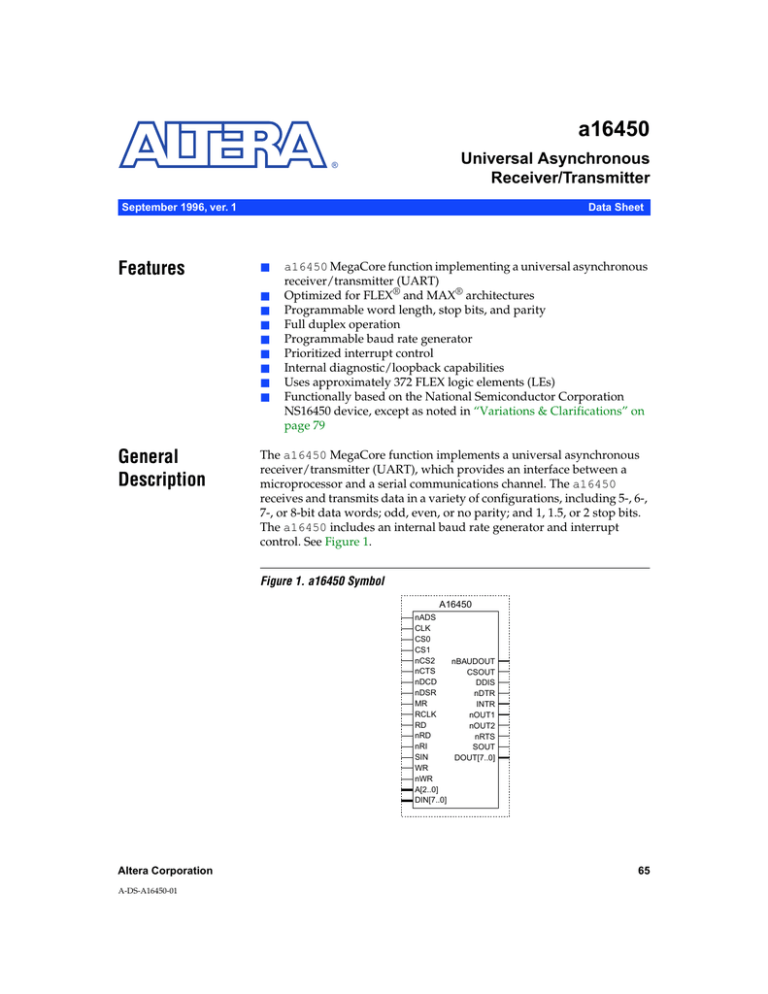
control. See Figure 1.
Figure 1. a16450 Symbol
A16450
nADS
CLK
CS0
CS1
nCS2
nBAUDOUT
nCTS
CSOUT
nDCD
DDIS
nDSR
nDTR
MR
INTR
RCLK
nOUT1
RD
nOUT2
nRD
nRTS
nRI
SOUT
SIN
DOUT[7..0]
WR
nWR
A[2..0]
DIN[7..0]
Altera Corporation
A-DS-A16450-01
65
a16450 Universal Asynchronous Receiver/Transmitter Data Sheet
Table 1 describes the input and output ports of the a16450.
Table 1. a16450 Ports (Part 1 of 2)
Name
Type
Polarity
Description
nads
Input
Low
clk
Input
–
cs0
Input
High
Chip select 0. The a16450 is selected when cs0, cs1, and ncs2 are
asserted, which permits read and write transactions to internal registers.
cs1
Input
High
Chip select 1. The a16450 is selected when cs0, cs1, and ncs2 are
asserted, which permits read and write transactions to internal registers.
ncs2
Input
Low
Chip select 2. The a16450 is selected when cs0, cs1, and ncs2 are
asserted, which permits read and write transactions to internal registers.
ncts
Input
Low
Clear to send. Indicates that the modem is ready to exchange data. A
change in input state from low to high is recorded in bit 0 of the modem
status register. If the modem status interrupt is enabled when ncts
changes state, an interrupt is generated. This input’s complement is
recorded in bit 4 of the modem status register.
ndcd
Input
Low
Data carrier detect. Indicates that the modem or data set detected a data
carrier. A change in input state is recorded in bit 3 of the modem status
register. If the modem status interrupt is enabled when ndcd changes
state, an interrupt is generated. This input’s complement is recorded in bit 7
of the modem status register.
ndsr
Input
Low
Data set ready. Indicates that the modem or data set is ready to establish
the communications link with the a16450. A change in input state is
recorded in bit 1 of the modem status register. If the modem status interrupt
is enabled when ndsr changes state, an interrupt is generated. This input’s
complement is recorded in bit 5 of the modem status register.
mr
Input
High
Master reset. Clears all registers (except the receiver buffer, transmitter
holding, and divisor registers) to their initial state. Resets control logic to
initial state.
rclk
Input
–
rd
Input
High
Read control. When rd or nrd is asserted and the a16450 is selected,
read transactions from internal registers are possible.
nrd
Input
Low
Read control. When rd or nrd is asserted and the a16450 is selected,
read transactions from internal registers are possible.
nri
Input
Low
Ring indicator. Indicates that the modem or data set detected the ring
signal. A change in input state is recorded in bit 2 of the modem status
register. If the modem status interrupt is enabled when nri changes state,
an interrupt is generated. This input’s complement is recorded in bit 6 of the
modem status register.
66
Address strobe. Enable signal to the address input receiver. The positive
edge of nads latches the register address bus into the address input
register.
Clock. Provides the master timing reference to the a16450.
Receiver clock. Operates at 16 times the baud rate clock.
Altera Corporation
a16450 Universal Asynchronous Receiver/Transmitter Data Sheet
Table 1. a16450 Ports (Part 2 of 2)
Name
Type
Polarity
Description
sin
Input
–
Serial data input. Receives data for the a16450.
wr
Input
High
Write control. When wr or nwr is asserted and the a16450 is selected,
write transactions to internal registers are possible.
nwr
Input
Low
Write control. When wr or nwr is asserted and the a16450 is selected,
write transactions to internal registers are possible.
a[2..0]
Input
–
Register address bus. Selects one of the internal registers. See Table 2.
din[7..0]
Input
–
Data input bus. The microprocessor writes to internal registers via the
din[7..0] bus.
nbaudout
Output
Low
Baud out. Transmitter clock that is controlled by the programmable baud
rate generator. Operates at 16 times the baud rate clock.
csout
Output
High
Chip select output. Indicates that the a16450 has been selected (i.e., the
cs0, cs1 and ncs2 inputs are asserted).
ddis
Output
High
Driver disable. Indicates that the microprocessor is reading data from the
a16450. This output is intended as a disable or direction control between
the a16450 and the microprocessor.
ndtr
Output
Low
Data terminal ready. Indicates that the a16450 is ready to exchange data.
This output is controlled by writing to bit 0 of the modem control register.
intr
Output
High
Interrupt. Indicates that an enabled interrupt condition has been met.
nout1
Output
Low
User-programmable output 1. This output is controlled by writing to bit 2 of
the modem control register.
nout2
Output
Low
User-programmable output 2. This output is controlled by writing to bit 3 of
the modem control register.
nrts
Output
Low
Request to send. Indicates that the a16450 is ready to exchange data. This
output is controlled by writing to bit 1 of the modem control register.
sout
Output
High
dout[7..0]
Output
–
Altera Corporation
Serial data out. Serial (transmitter) data out. When mr is asserted, the sout
output is asserted.
Data output bus.
67
a16450 Universal Asynchronous Receiver/Transmitter Data Sheet
Functional
Description
Figure 2 shows the a16450 block diagram.
Figure 2. a16450 Block Diagram
sin
rclk
Receiver Register
& Control
din[7..0]
a[2..0]
cs0
cs1
ncs2
nads
mr
rd
nrd
wr
nwr
ddis
csout
Receiver Buffer
Register
Decode &
Control
Logic
Output Data
Multiplexer
dout[7..0]
Baud
Generator
nbaudout
Transmitter
Register &
Control
sout
Modem
Control
Logic
nrts
ndtr
nout1
nout2
ncts
ndsr
ndcd
nri
Line Control
Register
Divisor Register
(MSB)
Divisor Register
(LSB)
clk
Line Status
Register
Transmitter Holding
Register
Modem Control
Register
Modem Status
Register
Interrupt Enable
Register
Interrupt ID
Register
68
Interrupt
Control
Logic
intr
Altera Corporation
a16450 Universal Asynchronous Receiver/Transmitter Data Sheet
Register Address Map
The state of the a[2..0] inputs determines which internal register the
microprocessor addresses. See Table 2.
The divisor register access bit (drab) allows access to the divisor register.
The drab is bit 7 of the line control register.
Table 2. Register Address Map
drab (1)
a2
a1
a0
0
0
0
0
Receiver buffer register—read only
Transmitter holding register—write only
1
0
0
0
Divisor register (LSB)
0
0
0
1
Interrupt enable register
Register
1
0
0
1
Divisor register (MSB)
X
0
1
0
Interrupt ID register
X
0
1
1
Line control register
X
1
0
0
Modem control register
X
1
0
1
Line status register
X
1
1
0
Modem status register
X
1
1
1
Scratchpad register
Note:
(1)
The X indicates “don’t care.”
Registers
The a16450 MegaCore function contains the following registers:
■
■
■
■
■
■
■
■
■
■
Altera Corporation
Receiver buffer
Transmitter holding
Divisor
Interrupt enable
Interrupt identification
Line control
Modem control
Line status
Modem status
Scratchpad
69
a16450 Universal Asynchronous Receiver/Transmitter Data Sheet
Receiver Buffer Register
The receiver buffer register is a read-only register that contains the last
complete data word sample received by the a16450.
Transmitter Holding Register
The transmitter holding register is a write-only register that loads the next
data byte to be transmitted by the a16450.
Divisor Register
The divisor register controls the programmable baud rate generator. The
16-bit divisor performs an integer frequency divide of the input clock. The
nbaudout output becomes the transmitter clock that operates at 16 times
the baud rate clock. For example, if the input clock is 10 MHz and the
divisor register is set to a binary 2 (0000000000000010), the nbaudout
will be a 5-MHz output with a 50/50 duty cycle. The effective baud rate
will be 1/16th of 5 MHz, or 312,500 baud. In addition, the nbaudout
output may be wrapped to the receiver section input clock (rclk) to
provide the receiver clock that operates at 16 times the baud rate clock.
The a16450 does not support a divide-by-0 operation, which produces
the same results as a divide-by-1 operation for the nbaudout output.
However, a divide-by-0 operation prevents the transmitter from
functioning because an internal signal, baud_en, is not generated. The
baud_en signal enables the clock in the transmitter.
Interrupt Enable Register
The a16450 supports interrupts from four different sources; the interrupt
enable register selectively enables or disables interrupts from each of
these sources. When a bit is reset to a logic low, the a16450 will not
recognize interrupts from that source. Table 3 shows the interrupt enable
register format.
70
Altera Corporation
a16450 Universal Asynchronous Receiver/Transmitter Data Sheet
Table 3. Interrupt Enable Register Format
Bit
Signal
Description
0
rda
Received data available. When set to a logic high, bit 0 enables
interrupts when receive data is loaded in the receiver buffer
register.
1
thre Transmitter holding register empty. When set to a logic high, bit 1
enables interrupts when the transmitter holding register is empty.
2
rls
Receiver line status. When set to a logic high, bit 2 enables
interrupts when the receiver line status register changes state.
3
ms
Modem status. When set to a logic high, bit 3 enables interrupts
when the modem status register changes state.
7..4
–
Read-only bits that are always set to a logic low.
Interrupt Identification Register
The a16450 has a priority encoding scheme for its four interrupt sources.
Table 4 shows the encoding scheme for each of the interrupts, their
priority, and the reset mechanism for each interrupt source. When set to a
logic low, bit 0 indicates that an interrupt is pending. Bits 1 and 2 indicate
the interrupt priority, and bits 3 through 7 are read-only bits that are
always set to a logic low.
Clearing an interrupt source does not affect any lower priority interrupts
that might be pending. When the interrupt identification register is
accessed, the highest priority interrupt at the beginning of the access is
recorded in the register. Other interrupts, including those of higher
priority, are recorded but are not recognized until the current register
access is complete.
Altera Corporation
71
a16450 Universal Asynchronous Receiver/Transmitter Data Sheet
Table 4. Interrupt Identification Register Format
Note (1)
Bit 0
Bit 1
Bit 2
Bits 7..3
Interrupt Type
Interrupt Source
Reset Mechanism
Priority
1
X
X
0
No interrupt
–
–
–
0
1
1
0
Receiver line
status
Overrun, parity, or
Read the receiver line Highest
framing errors; break status register
interrupt
0
0
1
0
Receiver data
available
Receiver data
available
Read the receiver
buffer
2
0
1
0
0
Transmitter
holding register
empty
Transmitter holding
register empty
Read the interrupt ID
register or write to the
transmitter holding
register
3
0
0
0
0
Modem status
cts, dsr, ri, or dcd Read the modem
change state
status register
4
Note:
(1)
The X indicates “don’t care.”
Line Control Register
The line control register sets the data and communication formats used by
the a16450. See Table 5.
72
Altera Corporation
a16450 Universal Asynchronous Receiver/Transmitter Data Sheet
Table 5. Line Control Register Format
Bit
Description
1..0
Word length control. Sets the length of the word associated with each transmitted or received word.
See Table 6.
2
Stop control bit. Controls the number of stop bits generated by the transmitter section. The receiver
circuitry checks for the first stop bit only, regardless of the state of bit 2. See Table 7.
3
Parity enable. When set to a logic high, parity generation in the transmitter section and parity
checking in the receiver section are enabled. The parity bit is inserted between the last word bit and
the first stop bit.
4
Parity even/odd. When set to a logic high, even parity is enabled; when set to a logic low, odd parity
is enabled.
5
Stick parity. Forces the parity bit to a known value. If parity is enabled and even parity is selected, the
transmitter section will transmit the parity bit as a logic low. Then, the receiver section checks that the
incoming parity bit is set to logic low.
6
Break control. When set, bit 6 forces the a16450 to transmit a break condition. The sout output is
forced to a logic low state for longer than one full word transmission. Disable the break by clearing
bit 6, which causes sout to return to a logic high. The sout output is set to a logic high upon master
reset.
7
Divisor register access bit (drab). This bit must be set high to access the divisor registers. A low
enables access to the receiver buffer and transmitter holding registers.
Table 6 lists the word length associated with bits 0 and 1.
Table 6. Word Length Control Format
Altera Corporation
Bit 0
Bit 1
Word Length
0
0
5 bits
1
0
6 bits
0
1
7 bits
1
1
8 bits
73
a16450 Universal Asynchronous Receiver/Transmitter Data Sheet
Table 7 lists the number of stop bits and word length associated with bit 2.
Table 7. Stop Bit Control Format
Bit 2
Word Length
Note (1)
Number of Stop Bits
0
X
1
5 bits
1
1.5
1
6 bits
2
1
7 bits
2
1
8 bits
2
Note:
(1)
The X indicates “don’t care.”
Modem Control Register
The modem control register controls the modem interface outputs.
Table 8 describes the modem control register format.
Table 8. Modem Control Register Format
Bit
Signal
Description
0
dtr
Data terminal ready. The user can program the dtr bit to control the ndtr output.
1
rts
Request to send. The user can program the rts bit to control the nrts output.
2
out1
Output 1. The user can program the out1 bit to control the nout1 output.
3
out2
Output 2. The user can program the out2 bit to control the nout2 output.
4
el
Enable loopback. When high, bit 4 causes the following:
■ The sout output is set to a logic high.
■ The sin input is disconnected (i.e., ignored).
■ The output of the transmitter shift register is internally connected (loopbacked) to the
receiver shift register input.
■ The modem control inputs are disconnected (i.e., ignored).
■ The modem control outputs are used internally in place of the modem control inputs.
7..5
–
Not used. These read-only bits are always set to a logic low.
Line Status Register
The line status register enables the host processor to examine data
transfers. Table 9 describes the line status register format.
74
Altera Corporation
a16450 Universal Asynchronous Receiver/Transmitter Data Sheet
Table 9. Line Status Register Format
Bit
Signal
Description
0
rdr
Receiver data ready. Indicates that an incoming word has been received and transferred to the
receiver buffer register. When bit 0 is set to a logic high, a receive data available interrupt is
generated. Bit 0 is cleared by reading the receiver buffer register.
1
oe
Overrun error. Indicates that new data wrote over unread data in the receiver buffer register.
When bit 1 is set to a logic high, a receiver line status interrupt is generated. Bit 1 is cleared by
reading the line status register.
2
pe
Parity error. Indicates that newly received data had incorrect parity. When bit 2 is set to a logic
high, a receiver line status interrupt is generated. Bit 2 is cleared by reading the line status
register.
3
fe
Framing error. Indicates that newly received data had an invalid stop bit. When bit 3 is set to a
logic high, a receiver line status interrupt is generated. Bit 2 is cleared by reading the line status
register.
4
bi
Break interrupt. Indicates that a break condition was detected on the serial input. A break
condition occurs when the serial data in (sin) is held at logic low for longer than one full word
transmission. When bit 4 is set to a logic high, a receiver line status interrupt is generated. Bit 4
is cleared by reading the line status register.
5
thre Transmitter holding register empty. Indicates that the a16450 is ready to accept a new data
word from the microprocessor for transmission. When bit 5 is set to a logic high, a transmitter
holding register empty interrupt is generated. Bit 5 is cleared by reading the interrupt ID register
or by writing to the transmitter holding register.
6
tre
7
–
Transmitter empty. Indicates that the transmitter holding register and the transmitter shift
register are both empty.
Not used. This read-only bit is always set to a logic low.
Modem Status Register
The modem status register enables the microprocessr to examine the
condition of the modem interface inputs. Table 10 shows the modem
status register format.
Altera Corporation
75
a16450 Universal Asynchronous Receiver/Transmitter Data Sheet
Table 10. Modem Status Register Format
Bit
Signal
Description
0
dcts
Delta clear to send. Indicates that the ncts input has changed state since the
processor last read the modem status register. When bit 0 is set to a logic high, a
modem status interrupt is generated.
1
ddsr
Delta data set ready. Indicates that the ndsr input has changed since the processor
last read the modem status register. When bit 1 is set to a logic high, a modem status
interrupt is generated.
2
teri
Trailing edge ring indicator. Indicates that a trailing (0 to 1) edge has occurred on the
nri input since the processor last read the modem status register. When bit 2 is set
to a logic high, a modem status interrupt is generated.
3
ddcd
Delta data carrier detect. Indicates that the ndcd input has changed state since the
processor last read the modem status register. When bit 3 is set to a logic high, a
modem status interrupt is generated.
4
cts
Clear to send. This bit is the complement of the ncts input.
5
dsr
Data set ready. This bit is the complement of the ndsr input.
6
ri
Ring indicator. This bit is the complement of the nri input.
7
dcd
Data carrier detect. This bit is the complement of the ndcd input.
Scratchpad Register
The scratchpad register is a general-purpose register provided for the
convenience of the user.
76
Altera Corporation
a16450 Universal Asynchronous Receiver/Transmitter Data Sheet
Timing
Waveforms
Figure 3 shows the read and write cycle waveforms for the a16450
megafunction.
Figure 3. Read & Write Cycle Waveforms
Write Cycle
clk
nads
a[2..0]
Valid
ncs2, cs1, cs0
Valid
csout
nwr, wr
Active
din[7..0]
Valid
Read Cycle
clk
nads
a[2..0]
ncs2, cs1, cs0
Valid
Valid
csout
nrd, rd
Active
ddis
dout[7..0]
Valid
Figure 4 shows the functional timing waveforms for the a16450.
Altera Corporation
77
a16450 Universal Asynchronous Receiver/Transmitter Data Sheet
Figure 4. a16450 Functional Timing Waveforms
Baudout Timing
clk
nbaudout (divide-by-1)
nbaudout (divide-by-2)
nbaudout (divide-by-3)
nbaudout (divide-by-n)
(n-2) clk cycles
2 clk cycles
Receiver Timing
sin
Start
Parity
Stop
Sample clk
intr (data ready
or receiver error)
nrd, rd
Active
Transmitter Timing
sout
Start
Data (5-8)
Parity
Stop (1-2)
Start
thre
nwr, wr
nrd, rd
Modem Control Timing
nwr, wr
rts, dtr,
out1, out2
cts, dsr, dcd
intr
nrd, rd
ri
78
Altera Corporation
a16450 Universal Asynchronous Receiver/Transmitter Data Sheet
Variations &
Clarifications
The a16450 differs from the National NS16450 device in the following
ways:
■
■
■
Altera Corporation
The bidirectional bus d[7..0] in the NS16450 is split into an input
bus din[7..0] and an output bus dout[7..0] in the a16450. The
dout[7..0] bus is the direct output of the output data multiplexer,
and is not tri-stated or otherwise affected by the rd or nrd inputs.
In the a16450 megafunction, the address registers are implemented
as registers, as opposed to latches in the NS16450 device. These
registers use clk as the clock source and nads as a clock enable.
The a16450 megafunction uses a single clk input as the primary
clock source. The NS16450 device uses the crystal oscillator interface
(xin input and xout output) as the primary clock source.
79
Copyright © 1995, 1996, 1997, 1998 Altera Corporation, 101 Innovation Drive,
San Jose, CA 95134, USA, all rights reserved.
By accessing this information, you agree to be bound by the terms of Altera’s
Legal Notice.
