Carbon Nanotube Inter- and Intramolecular Logic Gates
advertisement
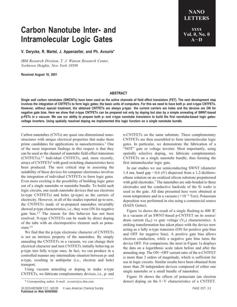
NANO LETTERS Carbon Nanotube Inter- and Intramolecular Logic Gates xxxx Vol. 0, No. 0 A-D V. Derycke, R. Martel, J. Appenzeller, and Ph. Avouris* IBM Research DiVision, T. J. Watson Research Center, Yorktown Heights, New York 10598 Received August 16, 2001 ABSTRACT Single wall carbon nanotubes (SWCNTs) have been used as the active channels of field effect transistors (FET). The next development step involves the integration of CNTFETs to form logic gates; the basic units of computers. For this we need to have both p- and n-type CNTFETs. However, without special treatment, the obtained CNTFETs are always p-type: the current carriers are holes and the devices are ON for negative gate bias. Here we show that n-type CNTFETs can be prepared not only by doping but also by a simple annealing of SWNT-based p-FETs in a vacuum. We use our ability to prepare both p- and n-type nanotube transistors to build the first nanotube-based logic gates: voltage inverters. Using spatially resolved doping we implemented this logic function on a single nanotube bundle. Carbon nanotubes (CNTs) are quasi one-dimensional nanostructures with unique electrical properties that make them prime candidates for applications in nanoelectronics.1 One of the most important findings in this respect is that they can be used as the channel of nanotube field-effect transistors (CNTFETs).2,3 Individual CNTFETs, and, more recently, arrays of CNTFETs4 with good switching characteristics have been produced. The next critical step in assessing the suitability of these devices for computer electronics involves the integration of individual CNTFETs to form logic gates. Even more exciting is the possibility of building logic gates out of a single nanotube or nanotube bundle. To build such logic circuits, one needs nanotube devices that use electrons (n-type CNTFETs) and holes (p-type) as the carriers of electricity. However, in all of the studies reported up to now, the CNTFETs made of as-prepared nanotubes invariably showed p-type characteristics, i.e., they were ON for negative gate bias.2,3 The reason for this behavior has not been resolved. N-type CNTFETs can be made by direct doping of the tube with an electropositive element such as potassium.5,6 We find that the p-type electronic character of CNTFETs is not an intrinsic property of the nanotubes. By simply annealing the CNTFETs in a vacuum, we can change their electrical character and turn CNTFETs initially behaving as p-type into fully n-type ones. In fact, we can produce in a controlled manner any intermediate situation between p- and n-type, resulting in ambipolar (i.e., electron and hole) transport. Using vacuum annealing or doping to make n-type CNTFETs, we fabricate complementary devices, i.e., p- and * Corresponding author. E-mail: avouris@us.ibm.com. 10.1021/nl015606f CCC: $20.00 Published on Web 00/00/0000 © xxxx American Chemical Society n-CNTFETs on the same substrate. These complementary CNTFETs are then assembled to form intermolecular logic gates. In particular, we demonstrate the fabrication of a “NOT” gate or voltage inverter. Most importantly, using spatially selective doping, we fabricate complementary CNTFETs on a single nanotube bundle, thus forming the first intramolecular logic gate. In our studies we use semiconducting SWNT (diameter 1.4 nm, band gap ∼0.6 eV) dispersed from a 1,2-dichloroethane solution on an oxidized silicon substrate prepatterned with gold electrodes.7 The nanotubes are side-bonded to these electrodes and the conductive backside of the Si wafer is used as the gate. All data presented here were obtained at room temperature and in a vacuum (<10-6 Torr). Potassium deposition was performed in situ using a commercial source (SAES Getter). Figure 1a shows the result of a single flushing to 400 °C in a vacuum of an SWNT-based p-CNTFET on its source/ drain current (IDS) vs gate voltage (VG) characteristics. A striking transformation has taken place with the device now acting as a fully n-type transistor (ON for positive gate bias and OFF for negative bias). A positive gate bias allows electron conduction, while a negative gate bias turns the device OFF. For comparison, the inset in Figure 1a displays the data on a logarithmic scale taken before and after the annealing step. The ON-OFF current ratio of the n-CNTFET is more than 3 orders of magnitude, which is sufficient for use in logic circuits. Similar results have been obtained from more than 20 independent devices composed of either one single nanotube or a small bundle of nanotubes. Figure 1b shows the effects of potassium (an electron donor) doping on the I-V characteristics of a CNTFET. PAGE EST: 3.3 Figure 1. Electrical characteristics of n-type nanotube FETs made by (a) annealing the device in a vacuum at 700 K for 10 min and (b) doping with potassium. The curves are obtained at different values of VDS starting at (a) 300 mV, step size 200 mV and (b) 200 mV, step size 200 mV. Doping produces n-type carbon nanotubes by shifting the Fermi level to the conduction band. As a result, the electron concentration in the conduction band increases and the conductance of the FET increases for a given positive gate voltage. Different groups have concluded that charge transfer from oxygen to the nanotube leads to p-doping.8-11 However, we find that the effects of O2 on the electrical characteristics of SWCNTs are distinct from those caused by doping the nanotube. For example, while doping is known to shift the threshold voltage for turning ON an FET,13 oxygen treatment of our samples shows no such threshold shift. Instead, oxygen exposure simply decreases gradually the electron conduction. Although doping may take place, it is the contact barriers that control the carrier injection. It appears that the dependence of these barriers on oxygen determines the electrical character of the CNTFETs.12 The two different methods used here to produce nCNTFETs, i.e., potassium doping and vacuum annealing, require vacuum and are reversed by exposure to air or oxygen. The problem of stability of the devices in air can, however, be solved by simply capping the nanotube with an B insulating film. In silicon technology, the need for capping has long been recognized because it ensures good stability over time and environment changes. In the case of nanotube devices, the requirements for the capping material are to be dense enough to prevent gas penetration at room temperature but permeable enough at high temperature to allow outgassing of the device through the cap. We first used PMMA as a capping material because it is a common resist that can be easily patterned. We found that a p-CNTFET protected by PMMA can be converted into an n-FET by annealing in a vacuum at 200 °C for 10 h. This n-FET is stable upon low oxygen exposure (10-2 Torr) but not under ambient air pressure. However, by using a thin silicon oxide layer (10 nm) for capping, we can produce air stable n-type devices.14 PMMA can also be used to provide an effective protection against potassium doping.6 By bonding together a p- and an n-FET, we have built the first logic gate based on carbon nanotube transistors, a “NOT” gate or voltage inverter. The NOT gate is a fundamental one in that, along with the “AND” gate, it can be used to generate all other logic gates. This inverter works exactly the same way as the ordinary CMOS inverters.15 Figures 2a-2d show the sequence of steps by which an intermolecular inverter (two independent CNTFETs are used) is fabricated using the vacuum annealing technique. First, one of the two CNTFETs is protected by PMMA, the other is not. After vacuum annealing, both CNTFETs are converted into n-CNTFETs. Next the device is exposed to 10-3 Torr of oxygen for 3 min. The unprotected n-CNTFET converts back to the original p-type, while the protected CNTFET remains n-type. In the completed circuit, the input voltage is applied simultaneously to the gates of the two complementary CNTFETs. The p-CNTFET is polarized by a positive voltage, the n-FET by a negative voltage. A common contact is used as the intermolecular inverter’s output. A positive input voltage turns the n-FET ON (the p-FET being OFF), resulting in the transmission of the negative polarization voltage to the output. A negative input, on the other hand, turns the p-CNTFET ON, inducing a positive output. In the intermediate input bias region, some current can flow through both FETs; that is, the device acts as a voltage divider. Thus, the transfer curve Vout(Vin) of this logic circuit is characteristic of a “NOT” logic gate, i.e., it changes an input of 1 or 0 to 0 and 1, respectively. The ultimate integration of CNTFETs would be to build logic gates using the same nanotube, i.e., produce an intramolecular logic circuit. We were able to implement this integration as shown in Figure 3a. This figure shows an atomic force microscope (AFM) image of a single-walled nanotube bundle deposited on top of three gold electrodes. As is shown schematically, the entire device is first covered by PMMA and then a window is opened using e-beam lithography. Potassium is used to n-dope half of the CNT through the window, while the other half remains p-type. The doping is adjusted so that the thresholds for switching of the p- and n-CNTFETs overlap. Figure 3b demonstrates that this design indeed leads to an intramolecular NOT gate. The ability to adjust the relative position of the two thresholds Nano Lett. Figure 2. Fabrication of a voltage inverter (“NOT” logic gate) using two nanotube FETs. Initially the two CNTFETs are p-type. One of them is protected by PMMA, the other is not. (a) After vacuum annealing both CNTFETs are converted to n-type. (b) The two CNTFETs are exposed to oxygen (10-3 Torr of oxygen for 3 min). The unprotected n-CNTFET (black curve) converts back to the original p-type, while the protected CNTFET (red curve) remains n-type. (c) The two complementary CNTFETs are wired as shown in the schematic. (d) Characteristics of the resulting intermolecular inverter (V ) (1.5 V) are shown. Figure 3. (a) AFM image showing the design of an intramolecular logic gate. A single nanotube bundle is positioned over the gold electrodes to produce two p-type CNTFETs in series. The device is covered by PMMA and a window is opened by e-beam lithography to expose part of the nanotube. Potassium is then evaporated through this window to produce an n-CNTFET, while the other CNTFET remains p-type. (b) Characteristics of the resulting intramolecular voltage inverter. Open red circles are raw data for five different measurements on the same device (V ) (2 V). The blue line is the average of these five measurements. The thin straight line corresponds to an output/input gain of one. by choosing the appropriate doping level allows a much sharper transition from the up to the down logic state. To use a logical gate as part of a more complicated computing system, a gain (output/input ratio) of one is Nano Lett. required. The intramolecular inverter presented here has a gain higher than one (1.6) and can thus be used to drive another gate or a more complicated logic circuit such as a ring oscillator. C In conclusion, we have discussed two different methods for the fabrication of n-type carbon nanotubes. Integrating n-type and p-type CNTFETs, we were able to demonstrate functional intermolecular and intramolecular inverters. These logic circuits have good output characteristics, and a gain larger than one is possible. In addition, our experimental findings suggest that the impact of oxygen on the electrical characteristics of tube devices is a contact effect rather than a bulk doping effect. Acknowledgment. We thank H.-S. P. Wong for useful discussions, B. Ek for expert technical assistance, and J. Bucchignano for help with e-beam lithography. References (1) Carbon Nanotubes: Synthesis, Structure Properties and Applications; Dresselhaus, M., Dresselhaus, G., Avouris, Ph., Eds.; SpringerVerlag: Berlin, 2001. (2) Tans, S.; Verschueren, A.; Dekker, C. Nature (London) 1998, 393, 49. (3) Martel, R.; Schmidt, T.; Shea, H. R.; Hertel, T.; Avouris, Ph. Appl. Phys. Lett. 1998, 73, 2447. D (4) Collins, P. G.; Arnold, M. S.; Avouris, Ph. Science 2001, 292, 706. (5) Bockrath, M.; Hone, J.; Zettl, A.; McEuen, P. L.; Rinzler, A. G.; Smalley, R. E. Phys. ReV. B 2000, 61, R10606. (6) Zhou, C.; Kong, J.; Yenilmez, E.; Dai, H. Science 2000, 290, 1552. (7) The oxide thickness is 140 nm. The gold electrodes are 300 nm wide, 30 nm thick, and separated by varying distances in the 200-800 nm range. (8) Collins, P. G.; Bradley, K.; Ishigami, M.; Zettl, A. Science 2000, 287, 1801. (9) Sumanasekera, G. U.; Adu, C. K. W.; Fang, S.; Eklund, P. C. Phys. ReV. Lett. 2000, 85, 1096. (10) Bradley, K.; Jhi, S-H.; Collins, P. G.; Hone, J.; Cohen, M. L.; Louie, S. G.; Zettl, A. Phys. ReV. Lett. 2000, 85, 4361. (11) Jhi, S.-H.; Louie, S. G.; Cohen, M. L. Phys. ReV. Lett. 2000, 85, 1710. (12) Martel, R., et al., unpublished data. (13) Sze, S. Physics of Semiconductor DeVices; Wiley-Interscience: New York, 1981. (14) Martel, R.; Derycke, V.; Avouris, Ph. AIP Conference Proceedings, Electronic Properties of NoVel Materials - Molecular Nanostructures; Kuzmany, H., Fink, J., Mehring, M., Roth, S., Eds.; AIP: Melville, New York, 2001. (15) Wese, N.; Eshraghian, K. Principles of CMOS VLSI Design; AddisonWesley: New York, 1988. NL015606F PAGE EST: 3.3 Nano Lett.
