SOFT PHOTOLITHOGRAHY-BASED FABRICATION PROCESS OF ON-CHIP
SOFT PHOTOLITHOGRAHY-BASED FABRICATION PROCESS OF ON-CHIP
SOLENOIDE-TYPE MICRO INDURCOTR FOR MICRO ENERGY
APPLICATION
Y. Zhang
*
, D. K. Lee, H. Hiroshima, T. Itoh, R. Maeda
Large Scale Integration Research Team, Research Center for Ubiquitous MEMS and Micro
Engineering/National Institute of Advanced Industrial Science and Technology (AIST), Tsukuba, Japan
*Presenting Author: yi.zhang@aist.go.jp
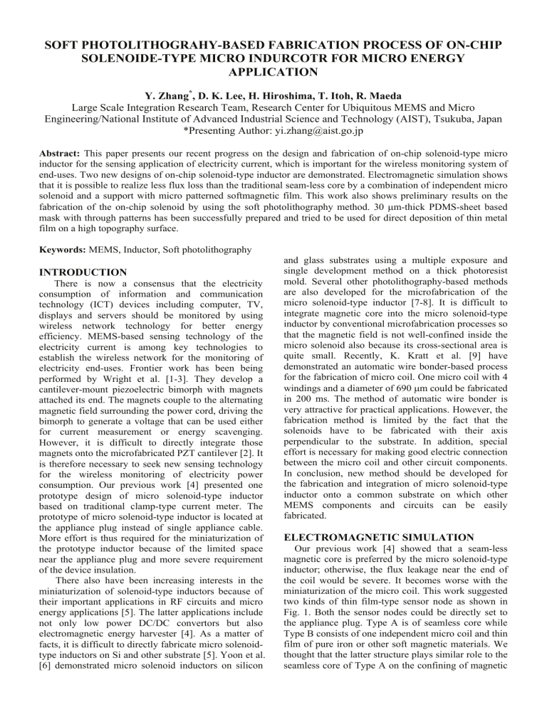
Abstract: This paper presents our recent progress on the design and fabrication of on-chip solenoid-type micro inductor for the sensing application of electricity current, which is important for the wireless monitoring system of end-uses. Two new designs of on-chip solenoid-type inductor are demonstrated. Electromagnetic simulation shows that it is possible to realize less flux loss than the traditional seam-less core by a combination of independent micro solenoid and a support with micro patterned softmagnetic film. This work also shows preliminary results on the fabrication of the on-chip solenoid by using the soft photolithography method. 30 μ m-thick PDMS-sheet based mask with through patterns has been successfully prepared and tried to be used for direct deposition of thin metal film on a high topography surface.
Keywords: MEMS, Inductor, Soft photolithography
INTRODUCTION
There is now a consensus that the electricity consumption of information and communication technology (ICT) devices including computer, TV, displays and servers should be monitored by using wireless network technology for better energy efficiency. MEMS-based sensing technology of the electricity current is among key technologies to establish the wireless network for the monitoring of electricity end-uses. Frontier work has been being performed by Wright et al. [1-3]. They develop a cantilever-mount piezoelectric bimorph with magnets attached its end. The magnets couple to the alternating magnetic field surrounding the power cord, driving the bimorph to generate a voltage that can be used either for current measurement or energy scavenging.
However, it is difficult to directly integrate those magnets onto the microfabricated PZT cantilever [2]. It is therefore necessary to seek new sensing technology for the wireless monitoring of electricity power consumption. Our previous work [4] presented one prototype design of micro solenoid-type inductor based on traditional clamp-type current meter. The prototype of micro solenoid-type inductor is located at the appliance plug instead of single appliance cable.
More effort is thus required for the miniaturization of the prototype inductor because of the limited space near the appliance plug and more severe requirement of the device insulation.
There also have been increasing interests in the miniaturization of solenoid-type inductors because of their important applications in RF circuits and micro energy applications [5]. The latter applications include not only low power DC/DC convertors but also electromagnetic energy harvester [4]. As a matter of facts, it is difficult to directly fabricate micro solenoidtype inductors on Si and other substrate [5]. Yoon et al.
[6] demonstrated micro solenoid inductors on silicon and glass substrates using a multiple exposure and single development method on a thick photoresist mold. Several other photolithography-based methods are also developed for the microfabrication of the micro solenoid-type inductor [7-8]. It is difficult to integrate magnetic core into the micro solenoid-type inductor by conventional microfabrication processes so that the magnetic field is not well-confined inside the micro solenoid also because its cross-sectional area is quite small. Recently, K. Kratt et al. [9] have demonstrated an automatic wire bonder-based process for the fabrication of micro coil. One micro coil with 4 windings and a diameter of 690 μ m could be fabricated in 200 ms. The method of automatic wire bonder is very attractive for practical applications. However, the fabrication method is limited by the fact that the solenoids have to be fabricated with their axis perpendicular to the substrate. In addition, special effort is necessary for making good electric connection between the micro coil and other circuit components.
In conclusion, new method should be developed for the fabrication and integration of micro solenoid-type inductor onto a common substrate on which other
MEMS components and circuits can be easily fabricated.
ELECTROMAGNETIC SIMULATION
Our previous work [4] showed that a seam-less magnetic core is preferred by the micro solenoid-type inductor; otherwise, the flux leakage near the end of the coil would be severe. It becomes worse with the miniaturization of the micro coil. This work suggested two kinds of thin film-type sensor node as shown in
Fig. 1. Both the sensor nodes could be directly set to the appliance plug. Type A is of seamless core while
Type B consists of one independent micro coil and thin film of pure iron or other soft magnetic materials. We thought that the latter structure plays similar role to the seamless core of Type A on the confining of magnetic
flux. Electromagnetic simulations have been performed by using Maxwell 3D simulator to calculate induction voltage of the micro coils upon the presence of AC current. The winding length of micro coil is set as 7.5 mm. The pitch is 75 μ m. The wire diameter is
50 μ m. The winding of the micro coil is 100 turns.
Pure iron ( μ r=4,000) and permalloy ( μ r=10,000) are used in the electromagnetic simulation. In order to examine the simulation results, small solenoid inductor was made by using 50 μ m-in-diameter copper wire on a 600 μ m-in-diameter permalloy wire. The home-made solenoid inductor was then set into a pure-iron plate to form a prototype sensor node. The prototype node was then loaded onto one appliance plug and its induction voltage was measured. Figure 2 shows the image of
Type A
the home-made solenoid on the appliance cord.
Figure 3 shows the measured induction voltage of the home-made solenoids and the calculated ones for different designs. There is noticeable difference between the measured and calculated value, suggesting that there is more loss than expected. The severe loss was found mainly through the ends of micro coils. The home-made node had the induction voltage of about
0.64 mV (V p
) upon the AC current of 4.5 A (I p
), which was enough for practical application. Higher induction voltage could be possible with improved design and fabrication. Figure 3 indicated that Type B is more sensitive than Type A. Considering that Type B is more suitable for mass production for low cost, it is superior to Type A. However, it is difficult to make such small micro coil by traditional technology for
Type B. Therefore, we are developing new microfabrication technology for the solenoid-type micro inductor by 3D exposure module [10] and conventional photolithography technology [11]. This work would mainly present preliminary experimental results on Type A also because it could be integrated with printing technology and other low cost processes.
5
Home-made solenoid
100 turns
200 turns
4
3
Type B_pure iron base
+permalloy core
Type B
_pure iron
2
Type A_pure iron
1
Type B
Figure 1 Schematic of micro solenoid-type inductor.
Figure 2 Image of a home-made solenoid supported by a pure iron plate for the measurement of induction voltage. The home-made solenoid is made of 50 μ m-in-diameter Cu wire:
100 turn; 6 mm long.
0
0 1 2 3 4 5 6
Current ( I p
) , A
7 8 9 10
Figure 3 Measured and simulated induction voltages.
EXPERIMENTAL
Type A is to be made on polymer sheet. 1 mmthick PMMA sheet is used as the polymer substrate because of its easy-to-imprint advantage.
Nanoimprinting technology is used for the preparation of the trench structure. The nanoimprinting process was performed at 70 o C under the pressure of about
300N by using a Si mold. The trench is about 310 um deep and 620 μ m wide for accommodate a permalloy core that has a 600× 600 μ m rectangular cross sectional shape. The core could be easily fabricated from permalloy sheet by mechanical method. However, it is difficult to form the required metal lines on such a
high topography surface by conventional lithography technology. Soft photolithography, which makes use of a flexible PDMS and other polymer mask, is usually used for the high topography substrate [12]. Figure 4 shows schematic of fabrication sequence for the flexible PDMS-based mask sheet. Firstly, a Si mold was prepared by using conventional photolithography process and dry etching method. Then the Si mold was treated by using CHF
3
plasma for easier peel-off operation. PDMS mixture (Sylgard 184@Dow
Corning, Co.) solution was spin-coated on the master substrate and covered by using a dummy wafer. Then it was cured at 70 o C for 1 hour under the pressure of about 0.3 MPa. There was still a very thin residual film on the top of the mold patterns so that the sample was dry etched in SF
6
for achieving through patterns. dry etching, those residual films had been removed. It was worthy to note that the surface roughness did not change after the dry etching.
Figure 5 Optical image of the PDMS mask sheet prepared in this work.
50 μ m
Figure 6 Optical images of the PDMS layer before and after the dry etching process.
Figure 4 Fabrication sequence of the flexible
PDMS-based mask sheet with through coil patterns. The low 3-D illustration shows that the
PDMS mask sheet is assembled onto the polymer substrate for the deposition of metal. (a) Si wafer;
(b) dry etching; (c) molding of PDMS layer; (d) dry etching of the PDMS layer; (e) Peel off the
PDMS sheet.
RESULTS AND DISCUSSION
Figure 5 shows the prepared PDMS mask that is about 30 μ m thick. It was free standing and easily handled during the assembly operation on to the nanoimprinted PMMA substrate. Figure 6 shows the surface of the PDMS mask before and after the dry etching. The colorful morphology was the residual
PDMS film in the through patterns. Their presence would be barrier to the deposition of Cu film. After the
50 μ m
Figure 7
Optical image of 2 μ m-thick Cu-film pattern formed by using the prepared PDMS mask sheet.
Figure 7 shows image of the formed 2 μ m-thick patterns on the PMMA sheet. 50 μ m-line width line had been successfully formed on the top surface.
However, it was failed to prepare continuous lines cross the trench structure mainly because the PMMA
sheet had deformed during the sputtering process owing to unsatisfied cooling. The fabrication process is under improvement.
CONCLUSIONS
New designs of micro solenoid-type inductor
(Type A and B) were demonstrated in this work. Type
B, which is a combination of a free-standing micro solenoid and patterned softmagnetic film, exhibited better sensitivity than Type A. The latter is a traditional seamless solenoid. It indicated that the effect of seam-less core could be realized by microfabrication technology. Preliminary experimental results of the home-made node exhibited enough sensitivity for practical application. We also introduced preliminary results on the fabrication of
Type A solenoid by using the soft photolithography method. 30 μ m-thick PDMS-sheet based mask with through patterns has been successfully prepared and tried to be used for direct deposition of thin metal film on the high topography surface.
REFERENCES
[1] Leland E S, Wright P K, White R M 2007 Design of a MEMS passive, proximity-based AC electric current sensor for residential and commercial loads Technical Digest PowerMEMS 2007
(Freiburg, Germany, 28
–
29 November 2007) 77
–
80
[2] Leland E S, Minor P, White R M, Wright P K
2008 A MEMS AC current sensor for residential and commercial electricity end-use monitoring
Technical Digest PowerMEMS 2008 (Freiburg,
Germany, 28
–
29 November 2007) 497
–
500
[3] Paprotny I, Leland E S, White R M, Wright P K
2009 Optimization of a die-sized (10X10Xmm 3 )
MEMS AC energy scavenger for residential and commercial electricity end-use monitoring
Technical Digest PowerMEMS 2009 (Freiburg,
Germany, 28
–
29 November 2007) 241
–
244
[4] Zhang Y, Lu J, Hiroshima H, Itoh T, Maeda R
2009 Simulation and design of micro inductor for electromagnetic energy scavenging at low
AC frequency in wireless sensor network
Technical Digest PowerMEMS 2009 (Freiburg,
Germany, 28
–
29 November 2007) 253
–
256
[5] Rebeiz G M 2003 RF MEMS Theory, Design and
Technology (John Wiley & Sons, Inc)
[6] Yoon J B, Kim B K, Han C H, Yonn E, Kim C K
1999 Surface mcrimachined solenoid on-Si and on-glass inductors for RF applications I EEE
Eelectron Device Lett. 20 487-489
[7] Joic K I, Ghantasala M K, Hayes J P, Jin H 2003
Fabrication of three-dimensional inductor coil using excimer laser micromaching J. Micromech.
Microeng.
13 782-789
[8] Chen Y E, Yoon Y K, Laskar J, Allen M 2001 A
2.4 gHz integrated CMOS power amplifier with micromachined inductors IEEE MTT-S
International Microwave Symposium Digest 67-
70
[9] Kratt K, Seidel M, Emmenegger M, Wallrabe U
2008 Solenoidal micro coils manufactured with a wire bonder Technical Digest MEMS 2008
(Tuscon, USA, 13-17 January2008) 996
–
999
[10] Zhang Y, Lu J, Mimura A, Matsumoto S, Itoh T
2010 MEMS-based exposure module for continuous lithography process on fiber substrates Technical Digest MEMS 2010 (Hong
Kong, China, 24-28January2010) 380
–
383
[11] Lee D K, Mekaru H, Hiroshima H, Matsumoto S,
Itoh T, Takahashi M, Maeda R 2010 3D UVmicroreplication using cylindrical PDMS mold,
Microsystem Technology 16 , 1399-1411
[12] Kim J G, Takama N, Kim B J, Fujita H 2009
Optical-softlithographic technology for patterning on curved surfaces J. Micromech.
Microeng. 19 055017

