Document 13995305
advertisement

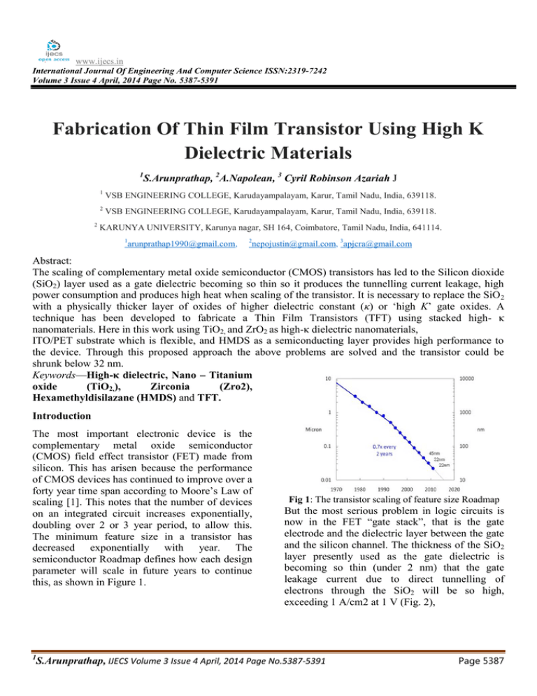
www.ijecs.in International Journal Of Engineering And Computer Science ISSN:2319-7242 Volume 3 Issue 4 April, 2014 Page No. 5387-5391 Fabrication Of Thin Film Transistor Using High K Dielectric Materials 1 2 S.Arunprathap, 2A.Napolean, 3 Cyril Robinson Azariah J 1 VSB ENGINEERING COLLEGE, Karudayampalayam, Karur, Tamil Nadu, India, 639118. 2 VSB ENGINEERING COLLEGE, Karudayampalayam, Karur, Tamil Nadu, India, 639118. KARUNYA UNIVERSITY, Karunya nagar, SH 164, Coimbatore, Tamil Nadu, India, 641114. 1 arunprathap1990@gmail.com, 2 nepojustin@gmail.com, 3apjcra@gmail.com Abstract: The scaling of complementary metal oxide semiconductor (CMOS) transistors has led to the Silicon dioxide (SiO2) layer used as a gate dielectric becoming so thin so it produces the tunnelling current leakage, high power consumption and produces high heat when scaling of the transistor. It is necessary to replace the SiO 2 with a physically thicker layer of oxides of higher dielectric constant (κ) or ‗high K‘ gate oxides. A technique has been developed to fabricate a Thin Film Transistors (TFT) using stacked high- κ nanomaterials. Here in this work using TiO2, and ZrO2 as high-κ dielectric nanomaterials, ITO/PET substrate which is flexible, and HMDS as a semiconducting layer provides high performance to the device. Through this proposed approach the above problems are solved and the transistor could be shrunk below 32 nm. Keywords—High-κ dielectric, Nano – Titanium oxide (TiO2,), Zirconia (Zro2), Hexamethyldisilazane (HMDS) and TFT. Introduction The most important electronic device is the complementary metal oxide semiconductor (CMOS) field effect transistor (FET) made from silicon. This has arisen because the performance of CMOS devices has continued to improve over a forty year time span according to Moore‘s Law of scaling [1]. This notes that the number of devices on an integrated circuit increases exponentially, doubling over 2 or 3 year period, to allow this. The minimum feature size in a transistor has decreased exponentially with year. The semiconductor Roadmap defines how each design parameter will scale in future years to continue this, as shown in Figure 1. 1 Fig 1: The transistor scaling of feature size Roadmap But the most serious problem in logic circuits is now in the FET ―gate stack‖, that is the gate electrode and the dielectric layer between the gate and the silicon channel. The thickness of the SiO2 layer presently used as the gate dielectric is becoming so thin (under 2 nm) that the gate leakage current due to direct tunnelling of electrons through the SiO2 will be so high, exceeding 1 A/cm2 at 1 V (Fig. 2), S.Arunprathap, IJECS Volume 3 Issue 4 April, 2014 Page No.5387-5391 Page 5387 design, all FET dimensions scale proportionately and the precise material does not affect electrical designs, so it is convenient to define an ‗electrical thickness‘ of the new gate oxide in terms of its equivalent silicon dioxide thickness or ‗equivalent oxide thickness‘ (EOT) as Fig 2: Leakage current vs. voltage for various thickness of SiO2 layers, The circuit power dissipation will increase to unacceptable values [2–4]. In addition it becomes increasingly difficult to produce and measure accurately films of such small thickness. Finally, the reliability of SiO2 films against electrical breakdown declines in thin films. Thus for these three reasons, but principally due to leakage, it is desired to replace SiO2 as a gate oxide. Tunnelling currents decrease exponentially with increasing distance. An FET is a capacitance-operated device, where the source-drain current of the FET depends on the gate capacitance, C=ε0KA/t (1) Where ε0 is the permittivity of free space, K is the relative permittivity, A is the area and t is the SiO2 thickness. Hence, the solution to the tunnelling problem is to replace SiO2 with a physically thicker layer of a new material of higher dielectric constant value, Figure 3. tox=EOT(3.9/K) tHiK. (2) Here 3.9 is the static dielectric constant of SiO2. The objective is to develop high K oxides which allow scaling to continue to ever lower values of EOT. The gate leakage problem has been apparent since the late 1990‘s [4], but then the criteria for the choice of oxide were not known. The choice of oxide narrowed to TiO2 and ZrO2. The material used as a semiconductor is an HMDS Hexamethyldisilazane which is an organic semiconductor material. The High-κ materials are provide high performance and low power CMOS applications beyond 32 nm. The facilitating of highperformance and low gate-leakage silicon and non-silicon transistor nanotechnology research via use of high-κ gate dielectrics and metal gate electrodes is attempted in this thesis work. The Thin Film Field Effect Transistors (TF-FET) are widely used in modern electronics devices. In this work, Figure 1 and 2 portrays the structure of TFT with high-k dielectric on an ITO/PET substrate. High- κ materials are having large thickness value, so we can shrinking the transistor below 32 nm and leakage current will be reduced. This TFET operates in high speed and consuming less power [6]. In flexible electronic applications the materials be deposited by using low-cost deposition methods. In addition, these materials have to be compatible with conventional at temperatures suitable for flexible substrates (< 150°C). Fig 3: Schematic of direct tunnelling through a SiO2 layer and the more difficult tunnelling through a thicker layer of high K oxide. This will keep the same capacitance, but will decrease the tunnelling current. These new gate oxides are called ‗high K oxides‘. For device 1 Fig 4: Schematic Diagram of the TFT with high- κ gate dielectric S.Arunprathap, IJECS Volume 3 Issue 4 April, 2014 Page No.5387-5391 Page 5388 Zirconia is an extremely refractory material. Pure zirconia exists in three crystal phases at different temperatures. Cubic structure (>2370°C), a tetragonal structure (1170 to 2370°C) and the monoclinic structure (below 1170°C). ZrO2 has been regarded as a high-k candidate for the semiconductor industry, because of their high dielectric constant of about 25, high melting point of 2700°C, and excellent chemical stability. Other properties of ZrO2 is high density, low thermal conductivity and high hardness. ZrO2 is classified as a wide band gap semiconductor and tends to become more conductive with increasing temperatures. Tio2 is also the high-κ dielectric material and its κ value is 80 [6] as well as higher band gap (~3.5 eV) [23]. It is also thermodynamically stable with HMDS. However the crystallization temperature is about 500o c, which is low for ulsi processing. Lucovsky et al., (2001) has reported that transition temperature can be improved by adding impurities into the film. Fig 5: SEM Image of Nano Zirconium Dioxide (Zro2) Experimental Details Preparation of Nano ZrO2 by Using Combustion Process The synthesis of the ZrO2 by Using Combustion process [7]. Since the Zirconia nitrate (Zro (No3)2), Glycine (NH2CH2COOH) are the raw materials used to synthesis the zirconia nanoparticles. Firstly, 2.3 g of the Zro(No3)2 is added in 0.83 g of Glycine and 5 ml distilled water is added, followed by 5 min of stirring with 400C. This mixed solution is kept in the furnace with 5500C and the solution is converted into foam product. This foam product contains ZrO2 and impurities. To remove the impurities the foam product is kept in 8000C at 6 hours we are getting pure ZrO2. Size of the zirconia nanoparticles are measured by using X-ray Diffraction (XRD), Scanning Electron Microscope (SEM) images. Fig. 5 and 6. Shows SEM and XRD image of the ZrO2 nanoparticles by prepared using Combustion process. 1 Fig 6: XRD Plot of Nano Zirconium Dioxide (Zro2) Preparation of Nano Tio2 by using sol gel technique Two-step method is the most widely used method for preparing Nano fluids. Nanoparticles, Nanofibers, Nanotubes and nanomaterials. In this method, first produced as dry powders by using chemical or physical methods. We used sol gel technique for preparation of nano Tio2 powders [8]. The obtained nano sized powder will be dispersed into a base fluid (Water) in the second processing step with the help of intensive magnetic force agitation. Size of the Titanium nanoparticles are measured by using X-ray Diffraction (XRD), Scanning Electron Microscope (SEM) images. Fig. 7 and 8. Shows SEM and XRD image of the Tio2 nanoparticles prepared by using sol gel technique. S.Arunprathap, IJECS Volume 3 Issue 4 April, 2014 Page No.5387-5391 Page 5389 Similarly, the device operates for the various gate voltages. Thus this fabricated field effect transistor act perfectly as a normal operation of a transistor. Fig 5: SEM Image of Nano Titanium Dioxide (Tio2) Fig 6: XRD Plot of Nano Titanium Dioxide (TIo2) Transistor Preparation. After preparing all the materials use Dip Coating or Doctor Blade any one method for coating Step 1: Take the ITO/PET substrate. Step 2: In that first coat the ZrO2 by Dip coating method. Step 3: TiO2 is coated by same method used for previous one. Step 4: HMDS is coated by doctor blade method. Step 5: Finally Source Drain and Gate terminals are fixed. Results and Discussion The gate voltage is kept constant and the graph is drawn between Vds and Id for Vds = 0V to 10 V. At constant gate voltage, the Vds vs Ids is drawn to obtain its knee voltage and to study the switching mode of the transistor. Figure 7 shows I-V characteristics of the Al2O3/ZrO2 TFT where the drain current, Ids, is plotted as a function of source–drain voltage, Vds, for different gate bias, VG. It can be seen that the device exhibits typical n-type field effect transistor characteristics with clear pinch-off and current saturation, indicating that the entire channel region under the gate metal can be completely depleted. When the gate voltage is 1.323V, the knee voltage is found to be 5.307V. Therefore, when the gate voltage is applied to 1.323V, IOFF state will be switched into ION state to 5.307V and vice versa. 1 Fig 7: I-V Characteristics of Vds vs Ids at Constant Vg Conclusion In summary, we reported the fabrication of a TFT with TiO2/ZrO2 gate dielectric. Then, fabricated field effect transistor is characterized at room temperature. The V-I characteristics are hence studied thoroughly. Threshold voltage Vt = 0.406V it shows that the performance of the FET is higher and consumes less power when compared to Silicon gate dielectric. In near future we plan to reduce the size of less than the proposed structure. Acknowledgment I am highly indebted to Mr Cyril Robinson Azaria J, Research scholar, Karunya University for his guidance as well as for providing necessary information. Mr Napoleon A, giving me an excellent guidance and support. I would like to express my gratitude towards my parents & member of VSB Engineering College for their kind co-operation and encouragement which help me in completion of this project. Reference 1. Cramming More Components onto Integrated Circuits. GORDON E. MOORE, LIFE FELLOW, IEEE Spectrum 2. G. Wilk, R.M. Wallace, J.M. Anthony, J. Appl. Phys. 89,5243 (2001) S.Arunprathap, IJECS Volume 3 Issue 4 April, 2014 Page No.5387-5391 Page 5390 3. R.M. Wallace, G.D. Wilk, Crit. Rev. Solid State 28, 231(2003) 4. R.M. Wallace, G. Wilk, MRS Bull. 27 (2002) 5. S.H. Lo, D.A. Buchanan, Y. Taur,W.Wang, IEEE Electr. Device L. 18, 209 (1997) 6. J. Robertson, ―High Dielectric Constant Oxides‖, J. Appl. Phys, 2004, Vol. 28, 265–291. 7. Qigen Wang, Ranran Peng, Changrong Xia, Wei Zhu, Huanting Wang,―Characteristics of YSZ synthesized with a glycine-nitrate process‖, Ceramics International, 2008, 34, 1773–1778 published online 10 august 2007. 8. Wen, D., and Ding, Y., Journal of Nanoparticle Research, 7 (2005), pp. 265– 274. Mr Cyril Robinson Azariah J. received his B.E. (Electronics and Communication Engineering) from the Anna University, Chennai in 2009 and M.Tech. (Nanotechnology) from Karunya University, in 2011. He is now working as an Assistant Professor in Electronics and Communication Engineering Department, VSB Engineering College, Karur, Tamilnadu. His area of research interest includes VLSI Technology, Integration Challenges of Nanotechnologies with CMOS Microelectronics Platform and Nano electronics Device Modelling. About Authors: Arun Prathap S is now a postgraduate student in M.E. Applied Electronics from the department of Electronics and Communication Engineering, VSB Engineering College, Karur, Tamilnadu. His area of research interest includes Nano electronics, CMOS VLSI Design, and Solid State Devices. Napoleon A. received his B.Sc. (Physics) from the Manonmaniam Sundaranar University, Tirunelveli. M.Sc. (Physics) from the Bharathiar University Coimbatore and M. Tech (Sensor System Technology) from Vellore Institute of Technology Vellore. He is now Assistant Professor in Electronics and Communication Engineering Department, VSB Engineering College, Karur, Tamilnadu. His area of research interest includes Nano Sensors, Microelectronics, and Optical Fibre Communication. 1 S.Arunprathap, IJECS Volume 3 Issue 4 April, 2014 Page No.5387-5391 Page 5391

