From: AAAI-83 Proceedings. Copyright ©1983, AAAI (www.aaai.org). All rights reserved.
TALIB:
An 16 Layout
Design
Jin Kim and John
Departments
In order to manage
the complexity
of large chip design
problems,
it has proven
useful
to take advantage
of the
hierarchical
structure
inherent
in most digital circuit designs
By utilizing
the hierarchical
structure,
the
[Mead
791.
complexity
of the chip design
problem
can be managed
by
into
less
complex
partitioning
the
original
problem
For
subproblems
at lower levels in the design
hierarchy.
example,
a chip floor
plan that partitions
the layout
into
functional
areas and constituent
cells can be prepared
at the
top level. With the chip plan as a guide, each functional
area
can
then
be constructed
from
cells
and
devices
in a
hierarchical
manner.
The functional
areas are subsequently
merged and fine adjustments
made to both the cells and the
chip floor plan until the cells are bound together
tightly.
This
paper
describes
a knowledge-based
system
for
automatically
synthesizing
integrated
circuit layouts for NMOS
cells.
The desired cell layouts are specified
in terms of their
general structural
and functional
characteristics.
From these
initial
specifications,
the
system
produces
correct
and
The system
performs
this task by
CoriJpact
cell layouts.
generating
plan steps at different
levels of abstraction
and
opportunistically
refining
each plan step at one level to more
specific steps at a lower level. Although
the implementation
of
this system has focused on NMOS technology,
the techniques
used are not restricted
to that technology.’
1. Introduction
I
.-
In recent
years
there
has been
a growing
interest
in
developing
systems
that automatically
synthesize
integrated
circuit
layouts
from high-level
functional
descriptions.
The
motivation
for developing
automatic
design synthesis
systems
is three-fold:
reduction
of design costs through
elimination
of
design errors, efficient
exploration
of the design space, and
reduction
in design time by allowing
designers
to work at a
higher level of abstraction.
This paper describes
a system,
called TALIB, that assists with the part of the IC synthesis
task
known as cell layout.
The program is implemented
in OPS5, a
general-purpose
production
system
language
[Forgy
771
[Forgy 811. TALIB accepts a description,
in netiist form, of the
schema.tic
of the NMOS digital circuit
to be laid out as input
and produces
the description
of the mask geometry
as output.
-
-
-
A typical integrated
circuit is implemented
on a silicon wafer
by creating,
through
a variety of fabrication
techniques,
layers
of different
substances
in geometric
patterns
on the wafer
The
superimposed
layers
of
conducting,
surface.
semiconducting,
and insulating
materials define the electronic
components
by interacting
through
different
layers.
The task
of laiiny
out an integrated
circuit
involves
determining
what
patterns on each layer will create the desired components
and
Interconnections.
For example.
in the NMOS technology
that
TALIB uses, a transistor
is created
whenever
a region on the
polysilicon
layer overlaps a region on the diffusion
layer. The
goal of the layout task is to put as much circuitry
as possible in
as small an area as possible.
Of course the resulting
circuitry
must work and satisfy the boundary
constraints
on ihe layout.
research
Corporation
The
views
authors
was
and through
and
conclusions
and should
either expressed
funded
National
or implled,
-
-
-
A
17
Figure
contained
in this document
as representing
of the Xerox Corporation
are those
of the
the official
policies,
or the National
Science
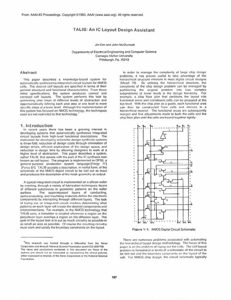
1 - 1:
NMOS
Digital
Circuit
Schematic
There are numerous
problems
associated
with automating
the hierarchical
layout design methodology.
The focus of this
paper IS on the problem of laying out the cells. The cell layout
problem is formulated
in terms of a schematic
of the circuit to
be laid out and the boundary
constraints
on the layout of the
cell.
For NMOS chip dcslgn,
the circuit
schematic
typically
through
a fellowship
from
the Xerox
Science Foundation grant ECS-8207709.
not bc interpreted
Science
Pa. 15213
Abstract
This
McDermott
of Electrical
Engineering
and Computer
Carnegie-Mellon
University
Pittsburgh,
1
Assistant
Foundation.
197
contains
a mix of logic gates and transistors
as shown
in
Figure l-1; the boundary
constraints
describe
the size of the
cell, its shape, the aspect ratio, and the ordering
of i/o signals
along the cell sides.
The boundary
constraints
reflect
the
characteristics
which the cell’s layout must have in order to fit
into the overall chip layout.
Solving
the cell layout problem
involves
generating
geometric
layout
patterns
for the circuit
schematic
which satisfy the boundary
constraints
as shown in
Figure l-2.
Further,
by using plans to control
focus,
[Sacerdoti
771.
TALlB
can
introduce
global
information
into
the
layout
generation
process.
Without the plan structure,
TALIB would
tend to search in a depth first manner by relying only on local
information.
Although
TALlL3 develops
and refines plans around objects
at various levels of abstraction,
most of its knowledge
is based
on empirical
rules that human experts utilize.
Because
TALIB
lacks any deep understanding
of the task domain,
it cannot
explain why its rules are valid.
2.1. Input Description
The input to TALlB consists
of two parts.
The first part
describes
the circuit components
and their interconnections.
A circuit is made up of devices and signal nodes.
A device is
any of the components
that are normally
present
in a digital
circuit such as NOT-gates,
NOR-gates,
and transistors.
Each
device has two or more terminals
by which it is connected
to
the rest of the circuit.
Two device terminals
are connected
to
each other through
a common
signal node.
The transistor
sizes in the circuit
schematic
can be specified
explicitly
or
default values can be generated
by TALIB.
The second
part of the input describes
the topological
and
geometric
requirements
around
the outside
boundary
of the
circuit layout.
The topological
information
includes
the order
in which
external
connections
must
appear
on the cell
This
requirement
can vary
in detail
from
a
boundary.
specification
of just the side of the cell on which a signal is to
be made available,
to a specification
of the exact ordering
which the signal node must have relative to other signal nodes
on that side.
The description
of each i/o signal can also
include
the layer on which the signal must be implemented.
The geometric
information
includes
the specification
of the
physical
parameters
of the cell layout; this can be stated in
terms of the upper bounds on the dimension
of the cell layout
or in terms of the cell’s aspect ratio.
The combination
of the
topological
and geometric
descriptions
of the cell layout make
up the boundary
constraints
of the cell layout problem.
The
output
of TALlB is the description
of the layout geometry
in
CalTech intermediate
Form (CIF) [Mead 791.
Figure
I-2:
NMOS
Layout
2. TALIB
The task of layout
generation
is that of placing
box-like
modules
on a plane bounded
on the X and Y axes, and
connecting
them by a set of wires according
to a given set of
rules.
In the process of planning
a layout, the designer
must
For
generate
intermediate
steps
based
on expectations.
example,
in placing
a subcircuit
on a layout
surface,
the
designer
must make assumptions
about how it wiil be laid out
in order to analyze
its impact on such global parameters
as
usage of metal channels
and total area; however,
the task of
actual
layout
of the subcircuit
cannot
be started
until its
placement
relative to other subcircuits
is known.
This facet of
tentative
reasoning
introduces
uncertainty
into the design
environment.
Since
such uncertainty
is inevitable
in binpacking
problems,
TALlB
is implemented
as a planning
system.
In addition
to
handling
uncertainties
in the
design
environment,
plans
are useful
in distinguishing
between
important
considerations
and details.
By utilizing
knowledge
at higher levels of abstraction,
TALlB can eliminate,
at an early
stage,
those
search
paths
that
are not
very
promising
2.2. Layout Models
TALIB
is capable
of limited
spatial
reasoning.
In the
degenerate
case when very little knowledge
can be brought
to
bear on a particular
region of the layout, TALlB expands
the
relevant
transistors
and their interconnections
in terms of
geometric
primitives
(e.g. rectangles)
within
the locality.
Inside the expanded
region, TALlB relies on a modified form of
the Lee expansion
routing algorithm
[Lee 611 to continue
the
layout process.
However,
the search space associated
with
even a small circuit can be very large when it is handled at the
geometry
level.
If all the details
of the search
space were
attended
to at this level, the combinatorics
would
enable
TALlB to solve only rather simple problems.
Therefore,
TALlB
represents
the state of the layout in terms of constructs
that
deal with subcircuits
rather than rectangles.
By working
with
abstractions
of the
layout
and
dealing
with
geometric
primitives
only when necessary,
TALlB is able to solve nontrivial problems efficiently.
The design
constructs
used by TALIB
are built around
subcircuits
that are commonly
found in digital NMOS circuits.
These subcircuits
are composed
of two to six transistors,
have
a small number of satisfactory
layout?,
and are usually used
many times in a design.
For each subcircuit,
TALIB creates a
collection
of objects
to represent
the characteristics
of the
subcircuit
instances
at different
levels of abstraction.
For
example,
a subcircuit
is represented
as a single object with its
estimated
layout area as one of its attributes
at one level of
abstraction,
as a set of partially
ordered
objects
that each
represent
a signal terminal
of the subcircuit
at a lower level of
abstraction,
and as a collection
of geometric
primitives
at a
still lower
level.
Associated
with
each
of the
objects
describing
a subcircuit
is a set of rules for updating
the
attributes
of the object.
In addition
to the above objects for describing
the state of
the design locally, there are global descriptors
that reflect the
general state of the layout.
These include objects that specify
the estimated
space for metal channels
under the given set of
boundary
constraints,
the number
of unused
channels,
the
maxirnurn
X and Y bounds,
and the amount
of space
remaining
in the X and Y dimension.
2.3. Knowledge
Organization
TALlR performs
the layout design task by utilizing
a large
knowledge
base of design heuristics
encoded
as rules.
The
rules ernbodying
the task specific
knowledge
can be roughly
classified
into two categories.
The bulk of TALlB’s
rules are
organized
around
the concept
of subtasks;
this type
of
organization
has proven
to be convenient
for capturing
knowledge
that has a relatively
narrow scope of applicability
[McDermott
821. The rest of TALlB’s
rules are demons
that
select subtasks,
detect their completion,
and detect constraint
violations.
Demons
have
been
useful
in other
task
environments
requiring
the
system
to react
quickly
to
changing
situations
[Haley 831.
In addition
to the subcircuit
based
constructs,
TALlB
maintains
a map of the layout surface
in terms of unused
areas.
Initially,
the
partitioning
of the
layout
surface
corresponds
to the number
of subcircuit
instances
in the
design.
As the design task proceeds,
additional
unused areas
will be generated
to reflect opportunities
for compacting
the
The adjacency
relationship
between
unused
areas
layout.
reflects
a particular
topological
style TALIB selects
to carry
out the layout.
The topological
style selected
depends
on the
initial
boundary
constraints
and on the complexity
of the
circuit.
The task of placing components
corresponds
to that
of mapping
subcircuits
or geometric
primitives
to one of the
unused areas.
The subtasks
known
to TALlB roughly
correspond
to the
steps in the plan developed
during the design process.
The
subtasks
are invoked
in a hierarchical
fashion
with those
handling
the more abstract
goals being expanded
in terms of
the more specific,
lower level, subtasks.
At the lowest level,
the primitives
in the subtask hierarchy
deal with generating
the
layouts for commonly
occuring
subcircuits
and with removing
unused
space
between
adjacent
subcircuit
layouts.
At a
higher level of abstraction,
subtasks
deal with placement
of
subcircuits
relative
to one
another
and
with
exploring
promising
areas on the layout surface.
Most of the subtasks
are familiar
to human experts,
but a few, like those dealing
with backtracking,
are almost never mentioned.
The version
of TALIB reported
in this paper knows how to perform
about
100 subtasks.
One exarnple
of a subcircuit-based
design construct
is the
circuit-layout
model.
For each circuit-layout
model, there are
a set of rules that fill in and update the attribute
fields of the
model.
The attribute
fields include
the estimated
X and Y
dirnensions
of the layout, the geometric
components
required
to realize the layout, the spatial relations
among the geometric
compon&ts,
and the orientation
of the components
in the
model.
Some of the attributes
of a circuit-layout
model for an
inverter are shown below.
TALlB’s
other rules, the demons, allow global knowledge
to
be brought
to bear whenever
it is relevant.
These rules have
four different
functions:
lnverter
{comment:
this is a circuit-layout
model for an inverter}
d) Classifying
Name
Status
X-dim
this
among
situations.
generates
subcircuits
A typical
adjacency
based
-type
-signal
o Creating,
typical
intantiating,
rule with
requirements
Pullup-type
Pullup-length
e Propagating
Pullup-width
Pullup-orientation
terminals
among
with
nature
interconnection
and updating
function
plan steps.
A
sets up precedence
plan steps.
constraints
A
another.
propagates
Pointer-to-pullup
this
rule
relationships
on the functional
of each subcircuit
and on the
characteristics
of the subcircuits.
Y-dim
Input-l
Input-l
design
function
from
typical
rule
distance
one
relations
of one subcircuit
subproblem
with
this
between
and those
to
function
signal
of another.
Pullup-pulldown-y-spacing
e Detecting
violation
this
function
process
2
A suitable
boundary
layout
subcircuit
will
vary
with
the
particular
constraints
199
the completion
in the
design-state.
detects
spacing
of tasks
and
A typical
the violation
rule for geometric
constraint
rule
with
of a fabrication
primitives.
result, though
rALlB typically generates
topological
plans that
are as good as those produced
by human experts,
the final
area of the ceil layouts IS 10 to 35 percent greater than those
Subsequent
versions
of TAI-lB
will
of human
designers.
improve upon this flgure,3 but we do not expect TALIB to ever
produce
cell layouts
that are consistantly
superior
to those
produced
by hurnan experts.
Most
of the knowledge
at lower
levels
of the subtask
hierarchy
is reliable
(i.e. if the current
state is on a solution
path, the state that results from applying
such a rule is almost
certain to be on the solution
path). The bulk of the knowledge
at higher
levels, however,
can only be applied
with limited
confidence
that
the
result
will lead
to a solution
(e.g.
knowledge
of how to cluster
and place subcircuits).
As a
consequence,
TALIB has to be able to backtrack.
The current
version
of TALlB consists
of about 1200 rules
with about 940 of these associated
with specific
subtasks.
It
has been used to generate
a variety of cell layouts for each of
a dozen circuits.
The most complex
of these circuits consists
of 36 transistors
with an ordering
specified
for the signals at
the cell boundary.
The circuit shown in Figure 1-1 is part of a
multiplier
slice and represents
one of the sirnpler circuits
laid
out by TALIB.
Since the boundary
constraints
on the circuit in
Figure l- 1 did not severely restrict the size of the layout, TALlB
was able to produce
the layout shown in Figure l-2 with fewer
Figure
2-1 shows
sorne
of the
than
2000
rule firings.
subcircuit
clusters
generated
by TALIB
during
its planning
process.
We are currently
refmlng TALlB’s
rule base and its
user interface
before
releasing
it for evaluation
to a small
community
of lC designers
at CMU.
Eventually,
TALlB
is
intended
to be part
of CMUDA,
a hierarchical
desibn
automation
system
for generating
complete
IC chips
from
behavioral
level specifications
[Parker 791 [Joobbani
821.
2.4. Control Cycle
The reasoning
process
is quite basic. with the selection
of
subtasks
being guided
by a set of domain-specific
control
rules.
The system reasons forward from the known facts and
its knowledge
about different
layout models to develop a plan
structure;
as soon as a plan, reflecting
the global interaction
among subproblems,
is developed
at one level, the plan steps
are expanded
in terms of those at a lower level of abstraction
in an opportunistic
fashion [Hayes-Roth
791.
Since
the
subtask
associated
with a particular
plan step is instantiated
by TALlB whenever
sufficient
information
is locally available,
TALIB occasionally
develops
isolated planning
islands that are
not on the solution
path.
This type of thrashing
is caused by
premature
introduction
of default information
and is minimized
through
the use of domain-specific
control
rules.
The
planning
process continues
until a solution
or a violation
of a
boundary
constraint
is detected.
If the later occurs,
the
system
backtracks
to undo
some
design
decision
and
attempts
an alternate
approach;
this involves
maintaining
and
analyzing
dependency
records to trace inconsistencies
back
to the appropriate
inferential
steps [Doyle 791.
TALlB’s
major
o Selecting
design
activities
design
constructs
boundary
constraints.
o Partitioning
the
layout
based on a particular
the spatial relationships
o Partitioning
topological
e Placing
different
the
are:
circuit
on
surface
the
into
basis
zones
of
and,
layout style, characterizing
among the zones.
netlist
in terms
of known
groupings.
topological
zones
groupings’
of the layout
of
subcircuits
in
surface.
u Refining
design
decisions
within
a particular
locality and propagating
design decisions
to other
parts of the partial
design.
Although,
there is a partial time ordering
among certain
parts
of the above design activities,
it is not possible to generate
an
a priori sequencing
plan for all the design activities.
This is
because
rnost of the activities
listed above are dependent
on
specific design situations.
Figure
2.5. Status of TALIB
In large chip designs, the bulk of the area savings are due to
the simplified
global routing
between
cells rather than as a
result of particularly
space efficient
cell layouts.
Based on this
3
observation,
we elected
to trade off reduction
in design time
(less search) against some inefficiency
in cell layout space as
a goal in developing
TALIB.
The version of TALlB reported
in
this paper reflects
this goal by basing the bulk of its design
activity around concepts.
the subcircuit
clusters,
that are at a
higher level of abstraction
than the geometric
primitives.
As a
Because
200
to the mdtvldual
be very dynamic.
In order
initial
TALKS
version
of
to follow
Although
usmg
particular
fabncntmn
conservative
Subciruit
a great deal of the domnm
closely coupled
constrained
2- 1:
these
knowledge
IC fnbricatlon
involved
to make
the knowledge
tractable,
allows
process.
design
for effective
it does
acqusillon
the
layout
rules reported
decouplmg
so only through
design rule set Ihat generally
in chip design
IIWS, this knowledge
reasonably
the Lambda-based
rules
Groupings
is
tends to
task for the
domain
was
in [Mead
791.
from
any
one
the use of a more
results in larger layout areas.
3. Conclusions
A knowledge-based
system for automatically
synthesizing
cell layouts has been described
in the context
of a hierarchical
The cell layout
task contains
a
chip design
environment.
number of NP-hard problems.
Unless the layout is based on a
tightly constrained
topological
style, such as PLAs or gatematrices,
the number
of alternatives
that must be explored
before
a candidate
solution
can be declared
acceptable
is
ordinarily
very large.
Based on the observation
that efficient
chip layouts
can be produced
without
locally
optimizing
the
layouts of the constituent
cells, a system for planning
design
steps around abstract layout concepts
has been developed.
[Lee 611
TALIB
has two basic strategies
which
help it limit the
amount
of search
required:
(1) It generates
plans and then
refines
them at several
levels of abstraction;
such planning
allows
it to identify
and tackle the least tractable
problems
first.
(2) Its plans are generated
on the basis of a variety of
features
of the circuit to be laid out; TALIB has a significant
amount
of knowledge
which
enables
it both
to quickly
generate
an abstract plan that is likely to be appropriate
and to
refine that plan to some extent before exploring
alternatives.
[Mead
C.Y.Lee.
An algorithm
for path connections
IRE Trans.
Electron.
September,
[McDermott
821
J.McDermott.
Rl: A Rule-Based
September,
C.Mead
791
to VLSI Systems.
A.Parker,
D.Thomas,
CMU Design
Autornation
[Forgy
771
system.
Artificial
Intelligence
12~~231-272,
Elsevier,
C.Forgy
and J.McDermott.
OPS, A Domain
System
Forw
811
Production
Language.
In 5th Joint
ACM,
Independent
1979.
Conf. Artificial
Intelligence.
1977.
C.L.Forgy.
OPS5 User’s Manual.
Technical
Report CMU-CS-81-135,
Carnegie-Mellon
[Haley
P.Haley,
831
University,
J.Kowalski,
1981.
J.McDermott,
R.McWhorter.
PTRANS: A rule-based
management
assistant.
Technical
Mellon
[Hayes-Roth
[Joobbani
791
821
Report
in preparation,
University,
Carnegie-
1983.
B. Hayes-Roth
and F. Hayes-Roth.
A Cognitive
Model of Planning.
Cognitive
Science 3:pp275-310,
1979.
R.Joobbani.
Know!edge-Based
PhD Thesis
University,
Chip Planning
Proposal,
System.
Carnegie-Mellon
1982.
201
G.Leive,
of Automated
Automation
and J.Kim.
System:
Conf..
1979.
for Plans and Behavior.
New York,
1977.
An
Data Path
E.D.Sacerdoti.
A Structure
References
J.Doyle.
A truth maintenance
771
DSiewiorek,
L.Hafer,
June,
[Sacerdoti
1979.
M.Barbacci.
In 7Gth Design
We wish to acknowledge
Dan Siewiorek
at Carnegie-Mellon
University
for the inspiration,
ideas,
and advice
he has
provided.
Also, we would like to thank Rick Barth and Don
Scharfetter
of Xerox
PARC and Art Krahmer,
Bill Mills, Ed
Snow, Doran Wilde, and Randy Young of Intel Corporation
for
their help in developing
TALIB’s knowledge-base.
vl9(9):pp39-88,
1982.
Addison-Wesley,
791
of Computer
and L.Conway.
Introduction
[Parker
:pp346-365,
Configurer
Systems.
Artificial
intelligence
Acknowledgements
791
Comput.
1961.
Example
Design.
[Doyle
and its
application.
IEEE,
