Phased-Array Antenna System for the MESSENGER Deep Space Mission
advertisement
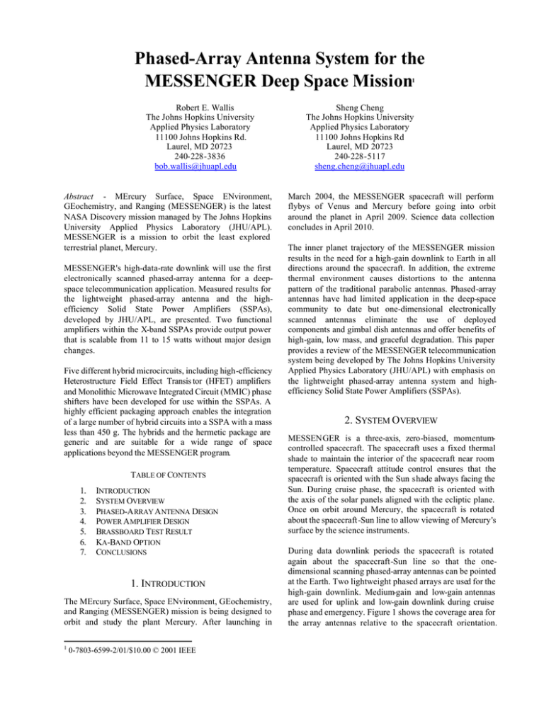
Phased-Array Antenna System for the MESSENGER Deep Space Mission 1 Robert E. Wallis The Johns Hopkins University Applied Physics Laboratory 11100 Johns Hopkins Rd. Laurel, MD 20723 240-228-3836 bob.wallis@jhuapl.edu Abstract - MErcury Surface, Space ENvironment, GEochemistry, and Ranging (MESSENGER) is the latest NASA Discovery mission managed by The Johns Hopkins University Applied Physics Laboratory (JHU/APL). MESSENGER is a mission to orbit the least explored terrestrial planet, Mercury. MESSENGER's high-data-rate downlink will use the first electronically scanned phased-array antenna for a deepspace telecommunication application. Measured results for the lightweight phased-array antenna and the highefficiency Solid State Power Amplifiers (SSPAs), developed by JHU/APL, are presented. Two functional amplifiers within the X-band SSPAs provide output power that is scalable from 11 to 15 watts without major design changes. Five different hybrid microcircuits, including high-efficiency Heterostructure Field Effect Transis tor (HFET) amplifiers and Monolithic Microwave Integrated Circuit (MMIC) phase shifters have been developed for use within the SSPAs. A highly efficient packaging approach enables the integration of a large number of hybrid circuits into a SSPA with a mass less than 450 g. The hybrids and the hermetic package are generic and are suitable for a wide range of space applications beyond the MESSENGER program. TABLE OF CONTENTS 1. 2. 3. 4. 5. 6. 7. INTRODUCTION SYSTEM OVERVIEW PHASED-A RRAY A NTENNA DESIGN POWER A MPLIFIER DESIGN BRASSBOARD TEST RESULT KA-BAND OPTION CONCLUSIONS 1. INTRODUCTION The MErcury Surface, Space ENvironment, GEochemistry, and Ranging (MESSENGER) mission is being designed to orbit and study the plant Mercury. After launching in 1 0-7803-6599-2/01/$10.00 © 2001 IEEE Sheng Cheng The Johns Hopkins University Applied Physics Laboratory 11100 Johns Hopkins Rd Laurel, MD 20723 240-228-5117 sheng.cheng@jhuapl.edu March 2004, the MESSENGER spacecraft will perform flybys of Venus and Mercury before going into orbit around the planet in April 2009. Science data collection concludes in April 2010. The inner planet trajectory of the MESSENGER mission results in the need for a high-gain downlink to Earth in all directions around the spacecraft. In addition, the extreme thermal environment causes distortions to the antenna pattern of the traditional parabolic antennas. Phased-array antennas have had limited application in the deep-space community to date but one-dimensional electronically scanned antennas eliminate the use of deployed components and gimbal dish antennas and offer benefits of high-gain, low mass, and graceful degradation. This paper provides a review of the MESSENGER telecommunication system being developed by The Johns Hopkins University Applied Physics Laboratory (JHU/APL) with emphasis on the lightweight phased-array antenna system and highefficiency Solid State Power Amplifiers (SSPAs). 2. SYSTEM OVERVIEW MESSENGER is a three-axis, zero-biased, momentumcontrolled spacecraft. The spacecraft uses a fixed thermal shade to maintain the interior of the spacecraft near room temperature. Spacecraft attitude control ensures that the spacecraft is oriented with the Sun shade always facing the Sun. During cruise phase, the spacecraft is oriented with the axis of the solar panels aligned with the ecliptic plane. Once on orbit around Mercury, the spacecraft is rotated about the spacecraft-Sun line to allow viewing of Mercury's surface by the science instruments. During data downlink periods the spacecraft is rotated again about the spacecraft-Sun line so that the onedimensional scanning phased-array antennas can be pointed at the Earth. Two lightweight phased arrays are used for the high-gain downlink. Medium-gain and low-gain antennas are used for uplink and low-gain downlink during cruise phase and emergency. Figure 1 shows the coverage area for the array antennas relative to the spacecraft orientation. The MESSENGER telecommunication system is designed to transmit the mission science data, receive spacecraft commands from Earth, and provide high-precision navigation data. As these are spacecraft-critical functions, the architecture for the telecommunication system must be redundant and immune from any credible single-point failure. The MESSENGER RF telecommunication system block diagram, shown in Figure 2, uses two Small Deep Space Transponders (SDSTs) cross-strapped to the forward and aft SSPAs. The SDSTs, manufactured by Motorola, provide the command, telemetry, and navigation capability. Figure 1. Phase-Array Antenna Coverage The broadside beams of the two opposing phased arrays are at 45° angles from the spacecraft-Sun line. As shown in the figure each phased-array antenna provides ± 45° scan capability. By rotating the spacecraft about the spacecraftSun line, full 4π steradian coverage is achieved. Within each SSPA are two functional amplifiers, which will be referred to as the distributed and lumped power amplifiers. The distributed power amplifier provides 1.4-W nominal drive level into each of the eight array antenna inputs. The lumped power amplifier provides an 11-W Xband output to the fan beam antenna and low-gain horn antennas. A set of RF switches following the diplexer allows either receiver or lumped SSPA to be connected with either forward or aft fan beams or low-gain antennas. This architecture provides cross-strapping for all components except for the distributed power amplifiers which are dedicated to their respective phased-array antennas. The distributed power amplifier provides a graceful degradation in case of an amplifier element failure. Even if a complete array failure occurs, on board solid-state recorders can store the science data for later downlink with the other array. Phased Array #1 TLM SSPA #1 SDST #1 LGA (-Y) Diplexer Exciter CMD’s Receiver Fanbeam (-Y) Hybrid Coupler Phased Array #2 Fanbeam (+Y) SSPA #2 TLM Exciter Diplexer LGA (+Y) LGA (+Z) Receiver CMD’s LGA (-Z) SDST #2 Figure 2. MESSENGER RF Telecommunication System System Performance Summary Table 1 provides a summary of the key characteristics for the JHU/APL MESSENGER phased-array communication system. In the SSPA functional area, we have integrated phased-array modules and a conventional SSPA with the efficiency and mass properties of existing X-band deep space SSPAs. Similarly, the 2.9-kg MESSENGER antenna compares favorably with traditional parabolic reflector technology. Single-axis -gimbal dish antennas with similar gain to the array, gimbal drive electronics, and launch lock mechanisms have an estimated mass of 4.5 to 6 kg. The MESSENGER phased-array antenna provides a mass advantage without the need for deployment mechanisms. Given a phased array SSPA output power of 41 dBm, cable losses of 1.0 dB, and an antenna gain of 27 dBic, the effective isotropic radiated power for the system is 67 dBm. Figure 3 shows the brassboard standing-wave array antenna comprised of eight waveguide "sticks" with 18 radiating slots cut in the narrow walls of the waveguides. Approximate dimensions for this array are 211 by 813 mm. Testing of the brassboard array at broadside and 45°-scan was facilitated by hand-trimming coaxial cables to produce the desired phase shift. Table 1. Phased-Array Performance Su mmary SSPA PCU Power amplifier subtotal Mass (kg) 0.45 1.50 1.95 Phased-array antenna Polarizer Array mounting plate Coax to waveguide adapters Radome Coaxial cables Antenna subtotal 0.58 0.32 1.23 0.08 0.32 0.40 2.93 Total 4.88 Component DC power (W) 42 10 52 52 3. PHASED -ARRAY ANTENNA DESIGN The severe thermal environment requires that the fixed thermal shade remain pointed at the Sun at all times. This restriction in spacecraft orientation precludes the use of a fixed high gain antenna and spacecraft maneuvering to achieve Earth pointing. However, rotation about the spacecraft-Sun line is still permitted. The ability of the spacecraft to rotate reduces the array scanning requirement from a two-dimensional scan to a one-dimensional scan. Array scanning in the broad beam plane requires the least number of cabled connections between the power amplifiers and the array and thus minimizes mass compared to narrow beam plane scanning. The onedimensional scanning in combination with spacecraft rotation allows an Earth downlink for all Sun-Earthspacecraft angles. In addition, the extreme thermal environment precludes the use of active radiating elements. Since the uplink data rate is typically very low, the phased array is needed for high-data-rate downlink only. Thus, the design requirements allow a relatively simple narrow-band, one-dimensional scan with no active radiating elements. Figure 3. Breadboard Phased Array Antenna (Dimensions: 211 by 813 mm) Figure 4 shows the measured antenna pattern at broadside and 45° beam scan. Scan loss at 45° was within a few tenths of a dB of the ideal –1.5 dB. The beamwidth of the array is relatively large (12 × 3°), which helps to minimize distortion due to thermal effects. The baseline flight array design uses 26 radiating slots, is approximately 211 by 737 mm, and has a projected mass of 580 g. An additional benefit of the array antenna for the downlink is its graceful degradation with failed amplifier modules. Numerical simulations have shown for a small number of failed modules, the effective isotropic radiated power (EIRP) is reduced by 20 log (m/n), where m is the number of working modules and n is the total number of modules. In the case of one failed amplifier module out of eight, this expression indicates a 1.16 dB reduction in EIRP. The medium-gain antenna (MGA) uses a single waveguide stick, like those in the array, to form a fan beam. The lowgain antenna (LGA) uses an open-ended waveguide antenna to provide broader beam width. More information on the LGA antenna is provided in [1]. Measured Antenna Patterns 30 Gain (dBi) 20 Radome 10 0 -10 -120 -80 -40 0 40 80 120 Angle Off Boresight (deg.) 0 Degree Scan 45 Degree Scan Figure 4. Breadboard Antenna Scan Pattern This reduction can be thought of as 0.58 dB less available transmit power and a 0.58 reduction in directivity or effective aperture area. The simulations have also shown that while the sidelobe levels increase with amplifier module failures, the direction of the beam is unchanged, therefore requiring no adjustment of the beam steering algorithm. The inherent polarization of the slotted waveguide array is linear polarization, which results in a 3-dB power loss when transmitting to the circularly-polarized Deep Space Network (DSN) ground stations. While the linearlypolarized array satisfies the mission science data rate requirements, a circularly-polarized array could double that data rate. To achieve this enhancement JHU/APL has researched techniques to produce circular polarization from a slotted waveguide array. Where possible we wanted to preserve the inherent advantages of the slotted array. These advantages include low mass, low loss, broad scanning capability, and high-temperature operation. We have focused our work on the design of external polarizers, which can be used with the slotted waveguide array. The baseline polarizer design uses parasitic radiating elements to produce circular polarization. This all-metal design is very tolerant of MESSENGER's wide temperature range and is easily manufactured. This design has shown promising results for a single waveguide stick, and we are proceeding with a full array implementation. Dielectric materials with very high operating-temperature characteristics have been identified for use in a meanderline polarizer. If significant problems are encountered with the parasitic element approach in the full array implementation, an alternative approach is the use of a multi-layer meander-line polarizer. The forward phased array transmits through an opening in the Sun shade. A radome, mounted to the Sun shade, must block sunlight, have good RF transmission characteristics over a ±45° angle of incidence, and have little performance change over the temperature range of –100 to +300°C. Finally it is highly desirable to have low polarization distortion to maximize the data return if circular polarization is implemented. This means that the horizontal and vertical components of amplitude and phase should track each other over scan angle and temperature. The design of the radome began with selection of thermal blanket materials with good transmission characteristics. Thermal blankets have inherent advantages. They are lightweight and space-qualified materials. A three-layer sandwich was investigated consisting of 0.25-mm-thick Nextel 312 cloth outer layers and an inner layer of Q-Fiber Felt. The felt is a low-density silica fiber material with low dielectric constant and loss tangent. The thickness of the silica fiber material is chosen to cancel reflections from the Nextel layers. Ideally this thickness is about a quarter wavelength, but this dimension is optimized with a genetic algorithm to provide good polarization tracking over the range of incidence angles. The chosen materials result in a very robust design. The dielectric constant and loss tangent of the silica fiber material are very low and change little with temperature. The thinness of the Nextel layers makes the design less sensitive to uncertainties or changes in its electrical properties. Figure 5 shows the predicted power transmission at 8.4 GHz as a function of the angle of incidence for horizontal and vertical polarization. Excellent loss and polarization tracking are shown for angles of incidence between 0 and ±45°. Subsequent measured data agreed well with the predicted data. 4. POWER AMPLIFIER DESIGN As previously described, each MESSENGER SSPA includes two different X-band power amplifier sections, i.e., a lumped power amplifier with a single 11-W output and a distributed power amplifier with eight 1.4-W outputs. Only one of these two amplifiers is powered, depending on the antenna selected. A digital controller receives beamsteering commands from the spacecraft main processor and provides the phase-shifter settings for the eight distributed power amplifiers. Lumped Amplifier MESSENGER Radome Power Transmission (%) 100% 98% 96% 94% 92% 90% 0 20 40 60 80 Scan Angle (Degrees) Horizontal Pol. 100 Vertical Pol. Figure 5. Radome Transmis sion Loss Versus Scan Angle This unit also transfers telemetry data from the SSPA to the spacecraft. A dedicated external power conditioning unit (PCU) supplies approximately 42 W of secondary DC power to the SSPA. The SSPA is mounted inside the spacecraft where the base plate temperatures are expected to be between –30 and +65°C. This temperature range is achieved using the Sun shade and passive radiators. A block diagram of the SSPA is shown in Figure 6. A parallel line coupler divides the input signal for the lumped and distributed amplifiers. The lumped amplifier consists of a Gallium Arsenide Monolithic Microwave Integrated Circuit (GaAs MMIC) amplifier, a 2.4-mm Heterostructure Field Effect Transistors (HFET) driver amplifier, and a power amplifier stage. Four MMIC power amplifiers, arranged in balanced configuration using a four-way divider/combiner, comprise the power amplifier stage of the lumped amplifier section. The same MMIC amplifier and HFET driver amplifier are used in the distributed amplifier. This arrangement is illustrated in the block diagrams by using different colors for different device types. The distributed amplifier starts with the MMIC amplifier followed by an eight-way divider. At each output of the divider are an MMIC phase shifter, two MMIC amplifiers, a 2.4-mm HFET driver amplifier, and a 4.8-mm HFET power amplifier. Isolators are used at all outputs of the SSPA to protect the power amplifier stages during testing as well as to ensure stable power amplifier performance. All active microwave devices used in the SSPA, including the MMICs and HFETs, are from Triquint. Both the lumped and the distributed amplifiers are expected to exhibit greater than 30% DC to RF efficiency while working at the specified output power level. To meet these requirements over the temperature range that will be Distributed Amplifier Figure 6. SSPA RF Section encountered, the SSPA design employs two temperature compensation schemes. The first scheme adjusts the DC supply voltage to the power amplifier stage as the temperature varies to compensate for the output powercapacity change of the power device. The other scheme uses a temperature-compensating attenuator to provide constant gain. Extensive temperature testing of the lumped and distributed amplifiers during the brassboard phase will be performed to collect data for the temperaturecompensation design. The nominal SSPA supply voltage is selectable to provide easy adjustment of the SSPA output power within the range of 11 to 15 W. Power Amplifier Packaging The MESSENGER SSPA packaging design leverages proven high-reliability microwave integrated circuit (MIC) and hybrid construction techniques to optimize mass, producibility and thermal path for the active devices. Maintaining a good thermal path allows minimum device operating temperature, which enhances performance and reliability. GaAs MMICs and HFETs are procured in die form and installed in hybrid microcircuits. The use of die form parts, as opposed to commercially available packaged parts, allows a wider range of parts to be considered, and allows device selection for optimum SSPA efficiency. As the packaging design was developed, careful consideration was given to the manufacturing and screening aspects of the circuits within the SSPA. Screening of the circuits consists of a sequence of electrical and environmental tests designed to eliminate devices which do not meet performance requirements. The traditional approach of using packaged semiconductors places the burden and risk of screening on the device supplier. The use of devices in die form required JHU/APL to consider the screening of the devices as an integral part of the microwave circuit design. Two fundamentally different approaches referred to as multi-chip and singlechip hybrids were considered. Descriptions of these approaches and the associated tradeoffs follow. The multi-chip module approach consists of one large hybrid assembly, which includes the lumped and distributed SSPA functions. A laser-welded hermetic aluminum chassis contains chip-and-wire-based microwave circuits. This approach results in the highest level of integration and results in the least mass and volume. In addition, the number of screened hybrids and test fixtures are minimized. However, with the higher level of integration comes increased non-recurring engineering (NRE) for the hermetic package and increased touch labor learning with a more complex hybrid. Since MESSENGER requires only two SSPAs, the reduced screening and recurring costs of this approach were outweighed by the increased development costs. A larger production volume is required for this approach to be economically attractive. Finally, placing the risk of screening failures at the end of the SSPA assembly sequence is highly undesirable in a schedule-critical program. The single-chip hybrid approach consists of single function hybrids containing only one active device. This approach requires a total of 47 hybrid circuits per SSPA. Figure 7 shows a versatile hybrid package, designed by JHU/APL, that accommodates each of the five circuit designs and enables integration of the hybrids into a high-density layout. By designing a single common hermetic package, NRE costs for the package and associated test fixtures are minimized. Since the hybrids contain very few components, assembly and screening yields are high. Any defects are discovered by screening after the minimum in elapsed schedule and value-added labor. Finally, the JHU/APL package and single-chip hybrids are generic and more likely to be reused in a wide range of space applications beyond the MESSENGER program than the custom multi-chip hybrid described previously. The singlechip hybrid is the chosen approach. 14.7 Kovar Ring Frame Tungsten -Copper Base Ceramic Feed Through and RF Lead 11.7 Ceramic Feed Through and DC Leads Figure 7. Microwave Hybrid Package Dimensions in mm As part of the tradeoff analysis between the multi-chip and single-chip hybrid approaches, a higher level packaging concept was needed for the single-chip hybrid approach. Figure 8 shows the layout of the SSPA. The layout shows a highly efficient integration of the lumped and distributed SSPAs functions, the hybrids that comprise them, and a digital controller. The mass estimate for this 260 by 130 by 13 mm assembly is 440 g. This mass compares favorably with the mass of existing X-band multi-chip hybrid SSPAs, which suggests that there need not be a mass penalty for the single-chip hybrid approach. Eight Distributed Amplifier Outputs Lumped Amplifier Output 130 Digital Controller Board Eight Way Divider Amplifier Input 260 Figure 8. SSPA Layout Dimensions in mm Power Amplifier Line-Up The MESSENGER SSPA design achieves high efficiency and small size without custom MMIC devices. The use of commercially available devices with established reliability allowed rapid development and verification of the hybrid circuit designs. Available packaged devices would not simultaneously meet the efficiency and output power requirements of the SSPA. MMIC and discrete die devices provide excellent performance, but the packaging, fabrication, and screening issues are often a deterrent to the SSPA manufacturer. These issues are minimized by using a small number of device types in the line-up and by re-using the devices throughout the line-up. The electrical design of the SSPA began by selecting suitable devices for the output stages, then working toward the inputs. Figure 9a shows the line up of one of the eight amplifier chains in the distributed amplifier. The output and driver stages are discrete MIC amplifiers, designed by JHU/APL, using the TGF4250 4.8-mm and TGF4240 2.4-mm HFETs, respectively. The supplier's data sheet for the 4.8-mm HFET shows 34 dBm output power and 53% power-added efficiency with +8 V drain bias. This device is operated at +6 V in order to reduce the total DC power consumption while maintaining high efficiency. Load-pull measurements were utilized when designing this output stage, as well as its driver. The 4.8-mm to 2.4-mm output to driver ratio of the amplifiers insures the driver stage has sufficient output power capacity when driving the final stage, making the amplifier less sensitive to gain variations versus temperature as well as life and normal device variations across the wafer lot. The 2.4-mm HFET is rated at 31.5 dBm output power and 56% efficiency with +8 V drain bias. This device is operated at +5 V in order to maintain high efficiency at the required output power. Driving the 2.4-mm HFET amplifier are two cascaded TGA8810 MMIC amplifiers. These amplifiers have 17 dB of gain and 17 dBm of output power. The TGP6336 MMIC is a five-bit phase shifter with 9-dB typical insertion loss. Only the first four mostsignificant bits of the phase shifter are necessary to provide less than 0.1 dB quantization loss while steering the phased-array antenna. These phase shifters require a singleended control signal for each phase shift bit. This was preferred over a complementary control signal interface, which would have required either more control lines into the hybrid package or more electronics within the package. A fixed attenuator, integrated into the phase-shifter hybrid package, helps to improve the output return loss of the phase shifter. A TGA8810 amplifier, shown in the SSPA block diagram (Figure 6), is used to drive an eight-way divider to form the complete distributed amplifier. Expected performance of the distributed amplifier is 12.3 W RF power, 37.9 W DC power, and 32% efficiency. Figure 9b is the line-up of the lumped amplifier. The output amplifier is a TGA 9083 MMIC amplifier capable of 8 W of output power and 35% power-added efficiency at +9 V. The initial line-up used only two of these devices in parallel to provide greater than 10 W combined output power. However, a desire to increase the output power and decrease the channel temperatures of these devices led to the current four-way combined configuration. These four parallel devices operate from a +7-V supply. Under this operating condition, the MMIC is capable of 5 W of output power and 40% efficiency. A TGA8810 MMIC amplifier followed by a TGA4240 amplifier drive the output stage. Expected performance of the lumped amplifier is 12.5 W total RF power, 37.8 W DC power and 33% efficiency. The most challenging part in the electrical design of the SSPA is achieving high efficiency, power, and gain in the two HFET amplifier stages. The manufacturer suggested output loads for high power and high-efficiency operation. A small signal model of the HFETs aided in the inputmatching circuit design. Large signal models were unavailable, and simulation of the amplifier in large signal operation was not possible. Instead, input-matching and output-matching circuits were designed using separate simulations. Initial circuits were assembled and tested, under large signal conditions, in a load-pull system. (a) TGP6336 TGA8810 TGF4240 TGF4250 (b) TGA8810 TGF4240 TGA9083 x4 Figure 9. SSPA Line-up, (a) 1/8 of the Distributed Amplifier Chain, (b) Lumped Amplifier The test results were used to adjust the circuit model, and new matching circuits were simulated. Final circuit designs were created that met the power, efficiency, and gain requirements. This procedure was applied to both 2.4-mm and 4.8-mm HFET amplifier designs. The low gate impedance of the HFETs causes some difficulty in the design process. At 8.4 GHz the gate impedance is outside the load-pull tuner's range. Designing a microstrip transformer to match the input impedance was challenging because of the uncertainty in the gate bondwire inductance. To reduce the number of the uncertainties in the design process, the initial amplifier circuits were comprised of input-matching and output-matching transformers and bond wires of a nominal length connected to the HFETs. The transistors were biased through external bias tees initially. Coarse adjustment of the circuits consisted of iterating the bond wire lengths. Fine-tuning was accomplished by removing the metalization of the microstrip transformer with a diamond scribe and by moving the parallel gate and/or drain bond wires closer together or farther apart. After the successful tuning of the transformers and bond wires, other essential parts of the amplifier were incorporated into a new design iteration. These included the RF chokes for bias injection, blocking capacitors, and a parallel line coupler. The coupler is intended for use as a diagnostic aid at the SSPA assembly level. While the addition of these circuit elements de-tuned the amplifier slightly, the above tuning procedure was repeated to realign the performance of the amplifier. Figure 10 shows the hybrid layout of the 2.4-mm amplifier. The differences between this and the 4.8-mm amplifier are the transformer dimensions and the resistor values in the bias networks. The drain bias circuit shown in the figure presents a very high impedance to the amplifier circuit at the operating 8.4 GHz frequency. A parallel resistorcapacitor circuit to ground improves the low-frequency stability. The gate-bias circuit is designed to present a 60 Ω load at DC to the gate and a slightly higher shunt resistance at 4.1 GHz to prevent sub-harmonic oscillations. All RF bond wires are nominally 27 mils long. TGF4240 factor as the custom package except that there are no walls and no lid. This construction method leverages JHU/APL's rapid prototype capability to determine the required dimensions for the hermetic package. Additionally the chip carrier method allows evaluation of hybrid circuits and the amplifier line-ups in a configuration that's very close to the final flight design. The engineering model will be a complete SSPA using parts, materials, and processes that are as close to those envisioned for flight as possible. Brassboard Stages Output Transformer Input Transformer Figure 10. Chip Carrier Layout of 2.4-mm Amplifier Four Way Divider/Combiner The design of the four-way combiner/divider circuit uses branch-line hybrid couplers in a two-level corporate configuration. The branch-line couplers provide excellent impedance match and amplitude balance with low loss in a microstrip medium. The couplers are fabricated on Rogers TMM10 material along with the other microstrip lines of the lumped amplifier. The use of a single board for these lines eliminates the need for tight tolerances and alignment of separate circuit carriers to the adjoining amplifier stages. Several samples of each of the devices were assembled and tested. All MMIC devices, including the TGA8810 MMIC amplifiers, the TGP6336 MMIC phase shifters, and the TGA9083 MMIC power amplifiers were found to perform in agreement with manufacturer's test data. The TGA9083 MMIC power amplifiers were tested at both +9 and +7 V. The TGA4240 HFET amplifiers were first tested with +8 V drain bias to verify that the devices meet the manufacturer's specifications. Then, the amplifiers were tested with +5 V drain bias and drive conditions consistent with the MESSENGER application. The amplifiers exhibited 10 dB of gain and 35.6% efficiency when driven to 25.6 dBm output power level. The TGA4250 HFET amplifiers were tested in the same manner. They were also found to meet the manufacturer's specifications when biased at +8 V. Testing with +6 V drain bias, they exhibited 7 dB of gain and 55.7% efficiency with 32.5 dBm of RF output power. Distributed Amplifier Brassboard Digital Controller The digital controller is comprised of three primary circuits: a 1553 remote terminal hybrid, an ACTEL field programmable gate array (FPGA), and an applicationspecific integrated circuit known as the Temperature Remote Input & Output (TRIO) chip. The digital controller receives the array steering information from the spacecraft main processor via a redundant MIL-STD 1553 bus and provides the eight phase shifters with a four-bit control word. The controller also utilizes this bus to transfer telemetry from the SSPA to the command and data handling system. Digital telemetry is provided to echo back the beam steering command. Analog telemetry data are converted to digital using the TRIO chip. For subassembly testing the phase shifters can be exercised without the digital controller through a separate test connector. A single chain of the distributed amplifier, as shown in Figure 9a, was assembled and tested at room temperature. A summary of the test results is shown in Table 2. Calculated efficiency of the entire distributed amplifier is 32% with 12.3 W total RF output power and 38.59 W total DC power consumption. This figure includes the single TGA8810 amplifier driving the eight-way power divider. These results for the first integrated assembly compare very well to the expected results. Table 2. Distributed Amplifier Single Chain Brassboard Performance RF output power: POUT Gain @ POUT 5. BRASSBOARD TEST RESULTS At the time of this writing, the MESSENGER SSPA development is near the completion of brassboard evaluation and the beginning of engineering model fabrication. In the brassboard phase of the project, the hybrids are assembled in an open chip carrier. This chip carrier has the same form RMS gain variation 1.5 31.9 36.2 W dBm dB ± 0.5 dB Gain compression @ POUT 2.2 dB Total DC power consumption 4.8 W 32.3 % ± 4.7 ° Efficiency RMS phase variation Brassboard Lumped Amplifier Measured room temperature results for the lumped amplifier brassboard, shown in Table 3, also compare favorably to the expected results. Table 3. Lumped Amplifier Brassboard Performance 12.6 41.0 39.5 W dBm dB 3.5 dB Total DC power consumption 36.4 W Efficiency 34.6 % RF output power: POUT Gain @ POUT Gain compression @ POUT 6. KA-BAND OPTION JHU/APL has begun development of critical components that would enable a 32 GHz high-gain downlink [2]. Specifically JHU/APL has designed Ka-band GaAs MMIC power amplifiers and phase shifters using the Triquint foundry process. Initial test results on these devices indicate power amplifier efficiency greater than 30%. This efficiency is sufficiently high for a viable Ka-band phased array. The motivation for this effort is that for the same antenna aperture and SSPA DC power used in the present X-band system, a Ka-band phased-array antenna could return two to three times the data rate. The projected improvement over X-band is despite increased atmospheric loss, increased radome loss, increased antenna pointing loss, and decreased SSPA efficiency. JHU/APL is currently studying the feasibility of inserting this technology into the MESSENGER program. 7. CONCLUSIONS The first electronically scanned phased array for deep space telecommunication is complemented by high-efficiency SSPAs in MESSENGER's telecommunication system being developed by JHU/APL. The one-dimensionally scanned phased array eliminates deployment mechanisms and offers a low mass solution relative to a two-dimensionally scanned array. A highly efficient, 11 to 15-W design has been developed using a modular assembly of hybrid microcircuits. The hybrids and the common hermetic package are suitable for a wide range of applications. This paper has described the design and provided measured data in these key areas of the system. The telecommunication system mass, DC power, and downlink data rate requirements have been met or exceeded because of these developments. Acknowledgements The MESSENGER program is sponsored by the NASA Office of Space Science. The authors wish to thank MESSENGER's Principal Investigator, Dr. Sean C. Solomon of the Carnegie Institution of Washington, and R. S. Bokulic, L. A. Ellis, R. C. Mallalieu, P. M. Malouf, W. P. Millard, J. E. Penn, M. R. Peterson, C. H. Ronnenburg, R. K. Stilwell, D. K. Srinivasan, and J. T. Will of JHU/APL for their support of this work. REFERENCES [1] Reinhart, M. J., Jensen, J. R., Cloeren J. M., DeBoy, C. C., Fielhauer, K. B., and Schulze, R. C., The CONTOUR Radio Communications System, IEEE 2001 Aerospace Conference Technical Digest. [2] Bokulic, R. S., Reinhart, M. J., Willey, C. E., Stilwell, R. K., Penn, J. E., Norton, J. R., Cheng, S., DeCicco, D. J., and Schulze, R. C., Advances in Deep Space Telecommunications Technology at the Applied Physics Laboratory, IAA 2000 Conference Technical Digest, paper IAA-L-1108. Robert E. Wallis is currently the Lead Engineer for the MESSENGER Phased-Array System. He received his B.S. from the Pennsylvania State University in 1980 and his M.S. from Villanova University in 1983, both in electrical engineering. He joined the JHU/APL Space Department in 1999. From 1983-1999, Mr. Wallis was with EMS Technologies, Inc. (formerly Electromagnetic Sciences Inc.) where he managed the Microwave Integrated Circuit (MIC) design group and led the development of switch matrices and SSPAs for spacecraft applications, including C-band SSPAs for the TOPEX mission, X-band SSPAs for the Mars98 and Stardust missions, and Ku-band SSPAs for the International Space Station. From 1980-1983, Mr. Wallis was with General Electric Space Systems Division in Valley Forge, Pennsylvania, as a member of the MIC design group. Sheng Cheng is currently the Lead Engineer for the MESSENGER SolidState Power Amplifier. He received his B.S. from the National Taiwan University in 1982 and his M.S. from The Johns Hopkins University in 1989, both in electrical engineering. He joined the JHU/APL Space Department in 1997 as a senior microwave circuit design engineer. From 1990 to 1997, Mr. Cheng worked at the Whiting School of Engineering of The Johns Hopkins University on the research and development of microwave circuit theory, design methodology and measurement techniques. Prior to that, Mr. Cheng was with the LKC Technologies in Gaithersburg, Maryland, as an electronic circuit design engineer.

