Recitation 9: MOSFET VI Characteristics
advertisement
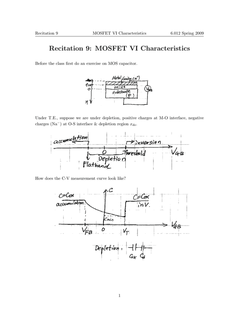
Recitation 9 MOSFET VI Characteristics 6.012 Spring 2009 Recitation 9: MOSFET VI Characteristics Before the class first do an exercise on MOS capacitor. Under T.E., suppose we are under depletion, positive charges at M-O interface, negative charges (Na− ) at O-S interface & depletion region xdo . How does the C-V measurement curve look like? 1 Recitation 9 MOSFET VI Characteristics 1 Ctot = Cox = 6.012 Spring 2009 1 1 + Cox Cd ox s , Cd = xd (VGB ) tox Useful relations: VFB = −(φgate − φbody ) 1 2s qNa (−2φp ) VT (n+ /p) = VFB − 2φp + Cox Cmin 1 = 2 Cox 1 + 2Cox (VT −VFB ) qs Na Where is Cmin ? When VGB changes, Cox does not change. Cd changes due to xd (VGB ). xd = 0 at VFB , xd = xd,max at VT =⇒ Cmin In tutorial, you can also find what the GV curves look like for p+ − n MOS or p+ − p MOS, or n+ − n MOS. MOSFET Device • We only talked about 2 terminals in our MOS capacitor. Where are the other terminals? Source/Drain. In the MOS capacitor, S/D tie to bulk → ground. Figure 1: MOSFET: 4 terminal device 2 Recitation 9 MOSFET VI Characteristics 6.012 Spring 2009 • As we mentioned, VGB =⇒ VG − VB . In MOSFET, we usually have, VDS = VD − VS VGS = VG − VS You can do manipulation: VGD = VG − VD = VGS − VDS • If the substrate of MOSFET is p-type, what type of MOSFET device this is? n-MOS or p-MOS? It is n-MOS. MOSFET operates when it is in Inversion. So for n-MOS: Source/Drain are n+ . Thus we have two p − n+ junctions between source-substrate (bulk), n+ (D) and p (B). When we apply biases, we try to keep VBS ≤ 0, VBD ≤ 0 otherwise the p − n+ junction will conduct. • When we use n-MOS, we always try to use source as reference: VGS , VDS etc. To start with, we let VBS = 0 =⇒ VGB = VGS From yesterday’s discussion or 6.002, what are the I-V characteristics (i.e. when applying VDS , what does IDS look like) of a n-MOS? 1. Remember we need to apply positive VGB (i.e. VGS here) in order to reach threshold. Before threshold, no conduction. =⇒ VGS < VT , IDS = 0 always (cutoff) 2. VGS ≥ VT , now we have inversion layer. If the VDS = 0, what is the inversion layer charge density? |Qn | = Cox (VGS − VT ) 3 Recitation 9 MOSFET VI Characteristics 6.012 Spring 2009 When VDS > 0, how will this charge density change? Now from S to D, along the channel interface, potential is no longer 0. V (y) = 0(0 < y < L) at each location y ∴, |Qn (y)| = Cox (VGS − V (y) − VT ) Decrease from source(y = 0)V (y) = 0 to minimum at D(y = L, V (L) = VDS ). To calculate IDS remember current ∝ charge density, ∝ carrier velocity. IDS = W · |Qn (y)| · vy (y) (vy (y) is velocity in the y direction at location y) How to calculate vy (y)? v = μ · E. So need to know Ey (y). How to know Ey (y)? Ey (y) = dV (y) (we have V (x, y) at each location: dy dV dx will give Ex ) Therefore to plug everything in the equation (1) IDS = w · Cox (VGS − V (y) − VT ) · μn · 4 dV (y) dy (1) Recitation 9 MOSFET VI Characteristics 6.012 Spring 2009 Integrating, y IDS dy = 0 IDS · y wμn Cox v(y) wμn Cox (VGS − VT − V (y )) dV (y ) 1 = (VGS − VT ) · V (y) − V 2 (y) 2 So we can solve the potential along each location y. V (y) = (VGS − VT ) − (VGS − VT )2 − 2IDS·y wμn Cox Since IDS should be the same everywhere, when y = L, V (y) = VDS , plug in (3) IDS = w VDS μn Cox (VGS − VT − ) · VDS L 2 When VDS is small, IDS (2) 0 w μn Cox (VGS − VT ) L ·VDS → linear Gate voltage controlled resistor Then as VDS increases, IDS bend over. When VDS = VGS − VT : IDS saturates IDSAT = w μn Cox · L 1 (VGS − VT )2 2 (only depend on VGS ) 5 (3) Recitation 9 MOSFET VI Characteristics 6.012 Spring 2009 PMOSFET Case Will need VBS ≥ 0, VBD ≥ 0 always. (typically VBS = 0). Now in order to have inversion: VGB = VGS < 0 In p-MOS, we use VSG = VS − VG > 0 VSD = VS − VD > 0 6 Recitation 9 MOSFET VI Characteristics 6.012 Spring 2009 When working with p-MOS, simply transform n −→ p VTn −→ −VTp IDn −→ −IDp VGS −→ VSG VDS −→ VSD w VSD μp Cox VSG + VTp − VSD VSD ≤ VSG + VTp Triode/linear: − IDp = L 2 w μp Cox (VSG + VTp )2 VSD ≥ VSG + VTp Saturation: − IDp = 2L 7 MIT OpenCourseWare http://ocw.mit.edu 6.012 Microelectronic Devices and Circuits Spring 2009 For information about citing these materials or our Terms of Use, visit: http://ocw.mit.edu/terms.

