6.012 MICROELECTRONIC DEVICES AND CIRCUITS
advertisement
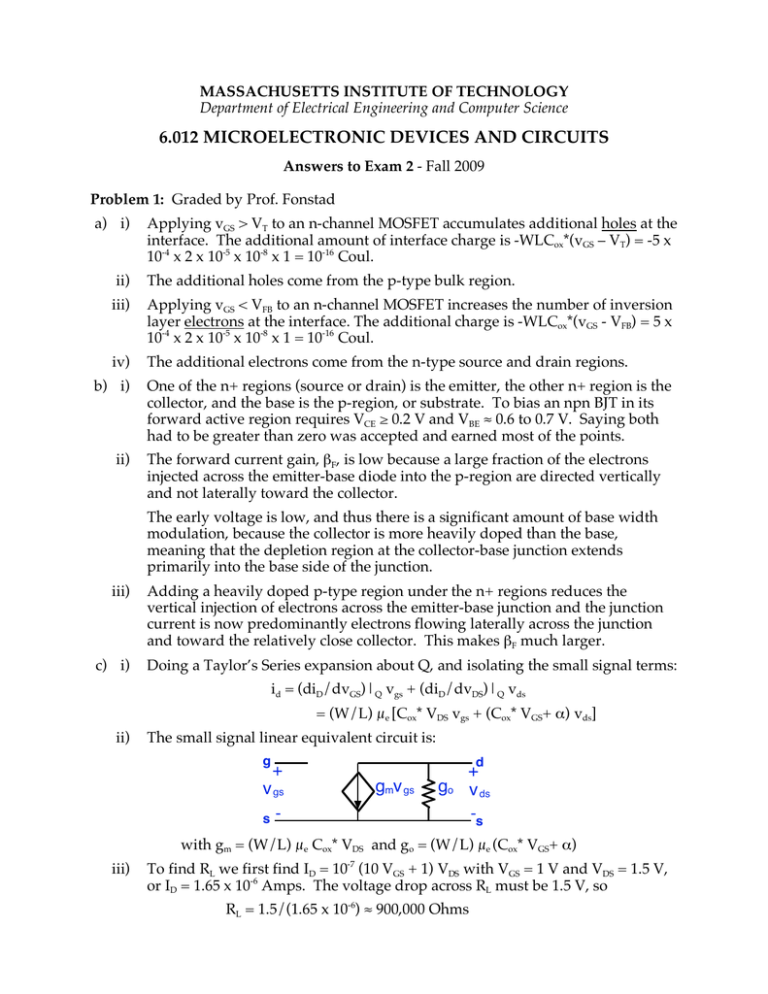
MASSACHUSETTS INSTITUTE OF TECHNOLOGY Department of Electrical Engineering and Computer Science 6.012 MICROELECTRONIC DEVICES AND CIRCUITS Answers to Exam 2 - Fall 2009 Problem 1: Graded by Prof. Fonstad a) i) Applying vGS > VT to an n-channel MOSFET accumulates additional holes at the interface. The additional amount of interface charge is -WLCox*(vGS – VT) = -5 x 10-4 x 2 x 10-5 x 10-8 x 1 = 10-16 Coul. ii) The additional holes come from the p-type bulk region. iii) Applying vGS < VFB to an n-channel MOSFET increases the number of inversion layer electrons at the interface. The additional charge is -WLCox*(vGS - VFB) = 5 x 10-4 x 2 x 10-5 x 10-8 x 1 = 10-16 Coul. iv) The additional electrons come from the n-type source and drain regions. b) i) One of the n+ regions (source or drain) is the emitter, the other n+ region is the collector, and the base is the p-region, or substrate. To bias an npn BJT in its forward active region requires VCE ≥ 0.2 V and VBE ≈ 0.6 to 0.7 V. Saying both had to be greater than zero was accepted and earned most of the points. ii) The forward current gain, βF, is low because a large fraction of the electrons injected across the emitter-base diode into the p-region are directed vertically and not laterally toward the collector. The early voltage is low, and thus there is a significant amount of base width modulation, because the collector is more heavily doped than the base, meaning that the depletion region at the collector-base junction extends primarily into the base side of the junction. iii) Adding a heavily doped p-type region under the n+ regions reduces the vertical injection of electrons across the emitter-base junction and the junction current is now predominantly electrons flowing laterally across the junction and toward the relatively close collector. This makes βF much larger. c) i) Doing a Taylor’s Series expansion about Q, and isolating the small signal terms: id = (diD/dvGS)|Q vgs + (diD/dvDS)|Q vds = (W/L) µe [Cox* VDS vgs + (Cox* VGS+ α) vds] ii) The small signal linear equivalent circuit is: g v gs d gmv gs go v ds s s with gm = (W/L) µe Cox* VDS and go = (W/L) µe (Cox* VGS+ α) iii) To find RL we first find ID = 10-7 (10 VGS + 1) VDS with VGS = 1 V and VDS = 1.5 V, or ID = 1.65 x 10⁻⁶ Amps. The voltage drop across RL must be 1.5 V, so RL = 1.5/(1.65 x 10-6) ≈ 900,000 Ohms We can now use this result and our linear equivalent circuit to draw the linear equivalent circuit for the full circuit, and from that we find the voltage gain: g d gmv gs v in = v gs go v ds = v out RL s s -6 -6 We find gm = 1.5 x 10 mho and go = 1.1 x 10 mho, and using the RL above we have 1/RL = GL = 1.1 x 10⁻⁶ mho. Thus, Av = vout/vin = -gm/(go+GL) ≈ - 0.7. Problem 2: Graded by Prof. Weinstein a) In flatband there is no depletion region, φ(0) = φn, and there is no voltage drop across the dielectric. "(x) "(0) = "n VFB = 1.5 "n -thi 0 !0.5 "n x L As indicated in the figure, VFB = 1.5 φn. b) At flatband the hole and electron populations are the same as they are in the bulk of the semiconductor. Thus, n(x = 0+) = ND, and p(x = 0+) = ni2/ND. c) At the onset of threshold φ(0) = -φn, the depletion region accommodates a change in potential of 2 φn and thus XD = [2εSi (2 φn)/qND]1/2. The potential drop across the dielectric qNDXDthi/εhi, and VT – VFB = - 2 φn – (thi/εhi)[2εSi (2 φn) qND]1/2. With these results, we find VT = VFB - 2 φn – (thi/εhi)[2εSi (2 φn) qND]1/2 = - 0.5 φn – (thi/εhi)[2εSi (2 φn) qND]1/2 The electrostatic potential profile at the onset of inversion: !(x) !n VFB = 1.5 !n -thi 0 "0.5 !n 2 !n XD !(0) = -!n VT (thi/#hi)(2#Si qND 2!n)1/2 L x The net charge distribution at the onset of inversion: !(x) qND qNDXD -thi 0 XD L x -qNDXD d) At the onset of inversion, the hole density at the interface is ND, i.e. p(x = 0+) = ND, and n(x = 0+) = ni2/ND. e) If there is a net sheet charge density, σi, at the interface, then at flatband there is a net sheet charge density, -σi, on the gate, and no other charge in semiconductor up to the interface. The voltage drop across the gate dielectric is σi(thi/εhi), and the flatband voltage must be more negative by this amount, ΔVFB = - σi(thi/εhi). The threshold voltage will be more negative by this same amount: ΔVT = - σi(thi/εhi). f) With an additional dielectric layer under the gate, there is additional voltage drop across the insulator for the same charge on the gate: ΔV (w.o. SiO2) = QG(thi/εhi) and ΔV (w. SiO2) = QG(thi/εhi) + QG(tox/εox). CG = QG/ΔV = 1/(thi/εhi + tox/εox) = εhi/2thi. Thus CG(w. SiO2)/ CG(w.o. SiO2) = ½. Problem 3: Graded by Prof. Palacios a) ID,sat = (Wmin/2Lmin)µe(εox/tox)(VGS - VT)2[1+λn(VDS-VDS,sat)] = [135/(2 x 35)] x 500 x (3.5 x 10-13/10-7) (0.6)2 (1+0.001(1-0.4))≈ 1.2 mA b) c) d) ro = 1/go = 1/λnID = 1/(10-3 x 1.2 x 10-3) = 10-6/1.2 ≈ 800,000 Ohms VIN1 VIN2 VOUT 0V 0V 1V 1V 0V 1V 0V 1V 1V 1V 1V 0V Wn, Inverter = 1 Wmin and Wp, Inverter = (µe/µh) Wn, Inverter = (500/200) Wmin = 2.5 Wmin e) We want the n-MOSFETs to each be minimum length since the effective length will be the sum of the lengths of two n-MOSFETs: Ln,NAND = 1 Lmin. and Ln,Eff = 2 Lmin. To minimize the delay, we will require the same current capability as in a standard inverter. To achieve this with an effective gate length Ln,Eff = 2 Lmin, the width needs to be Wn,NAND = 2 Wmin. As the current capability of the n-MOS branch is the same as in an inverter, the pMOS branch can be sized as in the inverter in question d). Thus CIN,NAND = 2.5WminLmin + 2WminLmin = 4.5 WminLmin. CIN,Inverter = WminLmin+ 2.5 WminLmin = 3.5 WminLmin, so CIN,NAND = 1.29 CIN,Inverter. f) The question speaks of inverter equivalents. The inverters have 15nA leakage if their output is high (n-MOS off), and 37.5 nA leakage if their output is low (pMOS, which is 2.5 x as wide, off) so the static power dissipation is 15 nA/gate x 1 V x 109 gates + 37.5 nA/gate x 1 V x 109 gates = 47.5 Watts! If you did the problem assuming 109 NAND gates, then the output is low, we have subthreshold current coming from each one of the two p-MOSFETs, which are connected in parallel. Therefore, the power dissipation is: 2 transistors/gate x 15 nA/transistor x 1 V x (1 x 109) gates = 30 Watts. When the output is high, the leakage current is due to the subthreshold current through the n-MOSFETs, which are connected in series and the current is dominated by one of them (i.e. they share the same current). Thus, the power dissipation in this state is: 1 transistor/gate x 15 nA/transistor x 1 V x (1 x 109) gates = 15 Watts. By adding the two contributions, the total dissipated power is: 30 W + 15W = 45 W g) i) Eave = 1 V/(35 x 10-7 cm) ≈ 3 x 10⁵ V/cm ii) The average sheet charge density is qn* = Cox*(vGS – VT) = 0.6 (εox/tox) = 0.6 x 3.5 x 10-6 = 2.1 x 10⁻⁶ coul/cm2. The current, iD = W qn* sch,ave. Assuming iD = 250 µA, we have: sch,ave = iD/(W qn*) = 2.5 x 10⁻⁴/(1.35 x 10-5 x 2.1 x 10-6) ≈ 0.88 x 107 cm/s. Assuming iD = 1.2 mA as found in part (a), we find: sch,ave ≈ 4.2 x 107 cm/s. iii) The current is almost 5 times smaller than the low field constant mobility model predicts because the velocity saturates at just under 107 V/cm. __________________________ Exam Statistics Average/Standard deviation: Problem 1 Problem 2 Problem 3 Total 21.5 19.2 25.1 65.8 5.3 7.6 5.5 14.9 Class median: 65 Distribution to nearest 5: Find your face in this picture 20 30 40 50 -σ 60 Total Score 70 Ave & Mean 80 +σ 90 100 MIT OpenCourseWare http://ocw.mit.edu 6.012 Microelectronic Devices and Circuits Fall 2009 For information about citing these materials or our Terms of Use, visit: http://ocw.mit.edu/terms.

