Document 13578690
advertisement
1
MASSACHUSETTS INSTITUTE OF TECHNOLOGY
Department of Electrical Engineering and Computer Science
6.012 MICROELECTRONIC DEVICES AND CIRCUITS
Problem Set No. 6
Issued: October 14, 2009
Due: October 21, 2009
Reading Assignments:
Lecture 10 (10/15/09) - Chap. 9 (9.3, 9.4)
Lecture 11 (10/20/09) - Chap. 10 (10.1.1a)
Lecture 12 (10/22/09) - Notes
Problem 1 - Do Problem 10.2 in the course text using a substrate doping level, NA, of 1 x
1016 cm-3 in Parts (a) thru (c) rather than 1 x 1017 cm-3, and assuming that the value of the
parameter α in the model developed in Lecture 11 is one (1). Also add the following
parts to this problem:
d) Consider building the same device with tox = 100 A . What must the doping level of
the substrate, NA, be to have the same threshold voltage you found in Part (a)? For
simplicity assume the flat-band voltage, VFB, is still -0.2 V, but after calculating the
new NA, find the actual flat-band voltage with this new doping level.
e) Repeat Part (b) and compare the answer for this new device with that of the original.
Problem 2 - This is a former exam problem (with all the work space and blanks removed),
so it won’t take you long to do.
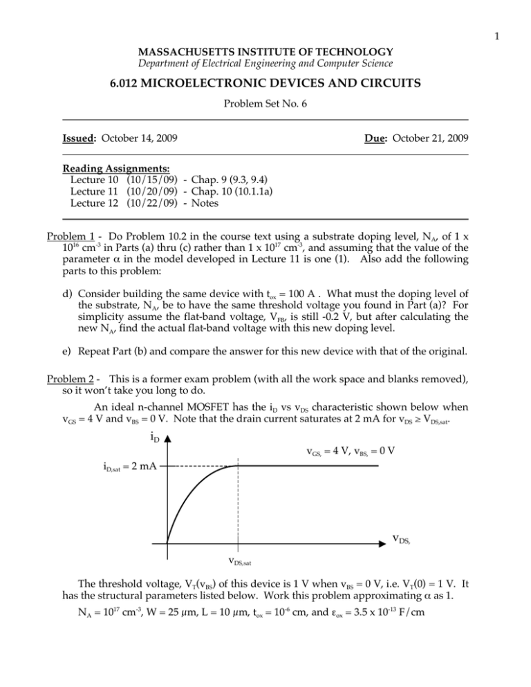
An ideal n-channel MOSFET has the iD vs vDS characteristic shown below when
vGS = 4 V and vBS = 0 V. Note that the drain current saturates at 2 mA for vDS ≥ VDS,sat.
iD
vGS, = 4 V, vBS, = 0 V
iD,sat = 2 mA
vDS,
vDS,sat
The threshold voltage, VT(vBS) of this device is 1 V when vBS = 0 V, i.e. VT(0) = 1 V. It
has the structural parameters listed below. Work this problem approximating α as 1.
NA = 1017 cm-3, W = 25 µm, L = 10 µm, tox = 10-6 cm, and εox = 3.5 x 10⁻¹³ F/cm
2
a) What is the drain-to-source saturation voltage, vDS,sat, when vGS = 4 V?
b) Use the information provided to calculate the electron mobility, µe, in the channel.
c) Find the inversion layer sheet charge density in the channel, qN*(y), at the source
end, i.e. qN*(0), and at the drain end, qN*(L), for the bias condition VGS = 4 V, VDS = 1
V, and VBS = 0 V.
d) Find the average net velocity, sy(y), of the electrons in the channel at the source end,
i.e. s y(0), and at the drain end, sy(L), for the bias condition in Part (c) above, for
which the corresponding drain current, ID, is 0.55 mA.
e) The drain-to-source voltage, vDS, is increased to 5 V, so that the bias condition is now
VGS = 4 V, VDS = 5 V, and VBS = 0 V. Find the inversion layer sheet charge density in
the channel, qN*(y), at the source end, i.e. qN*(0), and at the drain end, qN*(L) under
this new bias condition.
f) Next consider this MOSFET with a negative substrate-to-source bias, VBS. What is
the drain current of this device when it is biased in saturation, i.e., with VDS ≥ (VGS
VT), with VGS = 4 V and VBS = - 5 V? Suggestion: Calculate VT when VBS = -5V using
the expression below, and calculate iD in saturation with this new VT.
Threshold voltage expressions:
The definition of the threshold voltage of a MOSFET is:
VT (v BS ) " VFB # 2$ p#Si +
1
2%SiqN A 2$ p#Si # v BS
*
Cox
[
]
It is very common to write this in terms of VT(0), the threshold when vBS = 0, and
to introduce the parameter γ as shown below:
!
VT (v BS ) = VT (0) + "
with " %
{
2# p$Si $ v BS $ 2# p$Si
2&SiqN A
*
Cox
and
}
VT (0) % VFB $ 2# p$Si + " 2# p$Si
Problem 3 - This problem deals with the α factor in the gradual channel model for the
MOSFET (see for example the Lecture 11 Foils).
!
a) Calculate the α factor for the two device structures in Problem 1 above. Use your
results to recalculate the drain current, iD, in Parts (c) and (e) of that problem.
b) Calculate the MOSFET α factor for a device in which NAp is 5 x 1017 cm-3, and the
oxide thickness is 3 nm (3 x 10⁻⁷ cm). Take εox to be 3.5 x 10⁻¹³ F/cm and εSi to be 10
12 F/cm. Do this for back-to-source biases, v , of 0, -1, and -2 V.
BS
Problem 4 - Diode-like connections of MOSFETs are quite useful and important to
understand. Look at Figures 11.12 (a), (b), and (c) on page 351 in the course text.
Calculate and plot iD for vAB between 0 and 6 Volts using the device parameters given
in the figure caption. (These are curves a, b, and c in part e of this figure.)
MIT OpenCourseWare
http://ocw.mit.edu
6.012 Microelectronic Devices and Circuits
Fall 2009
For information about citing these materials or our Terms of Use, visit: http://ocw.mit.edu/terms.
