Homework #8 November 4, 2005
advertisement

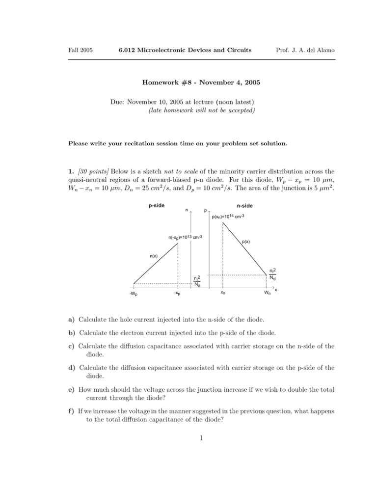
Fall 2005 6.012 Microelectronic Devices and Circuits Prof. J. A. del Alamo Homework #8 ­ November 4, 2005 Due: November 10, 2005 at lecture ( noon latest) (late homework will not be accepted) Please write your recitation session time on your problem set solution. 1. [30 points] Below is a sketch not to scale of the minority carrier distribution across the quasi­neutral regions of a forward­biased p­n diode. For this diode, Wp − xp = 10 µm, Wn − xn = 10 µm, Dn = 25 cm2/s, and Dp = 10 cm2 /s. The area of the junction is 5 µm2 . p-side n n-side p p(xn)=1014 cm-3 n(-xp)=1013 cm-3 p(x) n(x) ni2 Nd ni2 Na -Wp xn -xp Wn x a) Calculate the hole current injected into the n­side of the diode. b) Calculate the electron current injected into the p­side of the diode. c) Calculate the diffusion capacitance associated with carrier storage on the n­side of the diode. d) Calculate the diffusion capacitance associated with carrier storage on the p­side of the diode. e) How much should the voltage across the junction increase if we wish to double the total current through the diode? f ) If we increase the voltage in the manner suggested in the previous question, what happens to the total diffusion capacitance of the diode? 1 g) What is the ratio of the doping levels across the junction: Na/Nd ? h) In what direction should Na/Nd change if we wish to redesign the diode so as to get less diffusion capacitance at the same current level? (Assume that in redesigning the diode Dn , Dp , Wn − xn , and Wp − xp do not change). Choose one: Na/Nd must increase. Na /Nd must decrease. Explain. 2. [20 points] The equivalent circuit of a p+ ­n diode that you are trying to reverse engineer is measured at room temperature for two different bias points, one forward (I = 1 mA) and another one reverse (V = −10 V ). The results are sketched below: 2.6 nF 40 mS 2.9 fF I=1 mA V=-10 V Based on your understanding of the technology that has been used, you are pretty sure that you can assume that the diode is very abrupt (that is Na � Nd ) and that all minority carrier behavior is dominated by the lowly­doped side. On the microscope, you measure the area of the diode and you find it to be 10 µm2 . a) Estimate the doping level on the n side, Nd . b) Estimate the thickness of the n region, Wn . c) Verify whatever assumptions you needed to make. 3. [50 points] Design a family of Asymmetric Inverters As an additional step towards the 6.012 design project, in this problem you will simulate the dynamic behaviour of the CMOS inverter. After this homework assignment you will have all of the skills necessary to focus on the design of the project and use Cadence to the utmost. CMOS standard cells are collections of different types (inverter, NAND, DFF etc.) and sizes of CMOS gates. Different sizes of gates are designed to drive different sizes of capacitive loads with some nominal delay and rise time. In this homework we will extend the design of 2 our asymmetric inverter from the last homework into a family of inverters designed to drive three different sizes of capacitive load (50 f F , 150 f F , 500 f F ) with the same maximum delay (400 ps). Design a family of CMOS inverters. The DC behaviour must satisfy the following. The input range is 0 to 3.3 V . The output range is 0 to 5 V . The DC transfer function must have an output equal to 2.5 V when the input equals 1.65 V . The transient behaviour is as follows. For an input signal of a 1 M Hz square wave with rise and fall times of 1 ns, the delay (rising or falling) must be smaller than 400 ps. Design to obtain minimum power. In the last homework you designed an inverter that operated with an input from 0 to 3.3 V and an output from 0 to 5 V . Start from an inverter (Wp = 3 µm, Lp = 1.5 µm, Wn = 12.5 µm and Ln = 1.5 µm) which is designed so that Vout = 2.5 V when Vin = 1.65 V . Use Vdd = 5 V . Use the device models from the Cadence Tutorial. The minimum and maximum lengths are 1.5 µm and 100 µm with a 0.5 µm stepsize. The minimum and maximum widths are 3.0 µm and 100 µm with a 0.5 µm stepsize. a) [30 points] Describe a procedure in Cadence that allows you to size an inverter (Wp, Lp , Wn , Ln ) so that given a load capacitance CL and an input rise or fall time of 1 ns you achieve a maximum delay through the inverter of 400 ps or less and minimum power. Hint: Think about how you can change the delay of the inverter when the CL changes without changing the VM of the inverter. b) [10 points] Use your method to fill in the following table. CL 50 f F 150 f F 500 f F Note: Sinv = Wp Lp Wn Ln Sinv P ower tP HL tP LH Wp Lp Wn Ln Be sure to check that your inverter still has an output equal to 2.5 V when its input is 1.65 V . c) [10 points] Provide plots showing P ower, tP HL , tP LH to back up your claims. 3


