3.15 - Problem Set 4 Solutions Problem 1 a. b.
advertisement
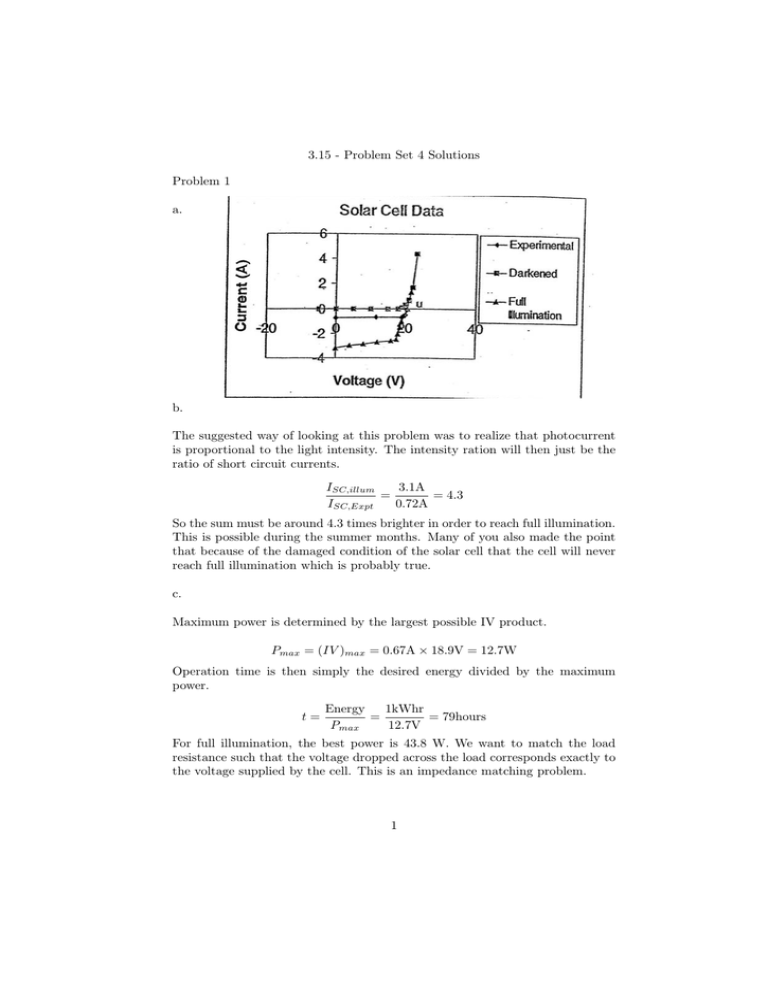
3.15 - Problem Set 4 Solutions Problem 1 a. b. The suggested way of looking at this problem was to realize that photocurrent is proportional to the light intensity. The intensity ration will then just be the ratio of short circuit currents. ISC,illum 3.1A = = 4.3 ISC,Expt 0.72A So the sum must be around 4.3 times brighter in order to reach full illumination. This is possible during the summer months. Many of you also made the point that because of the damaged condition of the solar cell that the cell will never reach full illumination which is probably true. c. Maximum power is determined by the largest possible IV product. Pmax = (IV )max = 0.67A × 18.9V = 12.7W Operation time is then simply the desired energy divided by the maximum power. t= Energy 1kWhr = = 79hours Pmax 12.7V For full illumination, the best power is 43.8 W. We want to match the load resistance such that the voltage dropped across the load corresponds exactly to the voltage supplied by the cell. This is an impedance matching problem. 1 Resistance is then found by taking the voltage at maximum power andd diving by current at maximum power. V 17.3V = = 6.8Ω I 2.53A For comparison, let’s take a 40W light bulb. Rload,opt = V2 V2 (120V )2 ⇔R= = = 360Ω R P 40W The optimal load of our solar cell is much less than for a typical light bulb. P = e. Connecting the 36 cells in series or parallel will change the voltage and current applied to the load. With the cells connected in parallel, Pmax is the same but V is 1/36 of the original value and I is 36 times the original value. Rparallel = Rseries = 5.3mΩ (36)2 In parallel, the cell can be used to power low impedance devices. f. The difference in current is due mainly to the large difference in juntion area between a diode and the solar cell. Current densities are roughly equivalent for both but the large area of the solar cell allows for a much larger current from relations V = IR and R = ρl/A. g. The J0 value ⇒ mobility is ≈ 900 cm2 /Vs. This is high ⇒ need good quality Si. 2 Problem 2 � � � � eV I = I0 exp −1 +Ig kT I0 = 10−6 A, Ig = −2 A (RP V + RL ) = V /I I (A) 2 0 0.5 1 1.5 1.7 1.8 1.9 V 0 0.38 0.37 0.36 0.34 0.33 0.317 0.299 IV 0 0 0.19 0.36 0.51 0.56 0.57 0.5 For I = 0: 10−6 exp eV − 10−6 − 2 = 0 kT 3 eV = 2 · 106 = 14.5 kT eV = 0.025 × 14.5 = 0.38V exp In general: � � 6 V = 0.025 ln 10 × (2 − I) I = 0.5A V = 0.37V Max power when I = 1.8A, V = 0.317, gives 0.57W. For load resistance: RP R + RL =0.317/1.8 = 0.18Ω ⇒ RL = 0.08Ω since RP R = 0.1Ω. b. Cell has limited efficienty. Solar spectrum has range of colors, and the higher energy photos waste all energy > Eg . Not all of surface can absorb light due to conductor lines. Not all light absorbed within Ln or Lp or juntion surface might be reflective. 4 Problem 3 There are many possible solutions to this problem. A number of factors must be considered: The principle of operation of a pin diode relies on a large amount of light being absorbed in the i-region, which means that this region should be wirder than any other layer throught which light passes. However, a shorter Wi will enable charge carriers to cross the region in less time. fmax ∝ W1i When used in conjuntion with a resistor, an RC time constant also affects the frequency response ∝ Wi (considering the pin structure to be similar to a ca­ pacitor). The device will operate at frequencies up to a certain cut-off, limited by those considerations. Devices of smaller width may have trouble absorbing longer wavelengths. To compensate for this, we can employ materials layers that help confine the light to the i-region by reflection. Device doping must be arranged such that during operation, the entire i-region is depleted. One possible solution is given as follows: If we assume ND = 1010 cm−3 in the n-region and NA = 1019 cm−3 in the pregion, then we see that the i-region will deplete under � the application of a small reverse bias. Considering the p+ -i junction, xd = ⇒ V ≈ 3.3 volts. 2ER E0 4ND (Vbi − V ); xd ≈ 23µm We will the set the n+ and p+ regions to be short, to reduce light absorption, but long enought to support i-deplection. Wn+ = Wp+ = 1µm. Neglecting adsorption of incident light in the p+ /n+ regions, and assuming that incident photons are contained by the internally reflective layers, the wavelength range over which this device is effective is determined by the band structure. The optimum wavelength will be just lower than λg = 1.24 Eg = 1µm. 5 The expected frequency response will attenuate signals above the cut-off fresat quency fmax = VW = 4.4GHz. i To estimate minimum detectable light intnesity, note that the photogener­ ated current must exceed the minimum current that can be detected by whatever device we use to measure it. This will be limited by noise in the system. If we assume a typical minimum current of Imin = 10−7 A, then the corresponding light intensity is given by: coulombs e-h pairs = q(n + p) second second nph = n = p = # photons nph = 6.25 · 1011 second nph photons = 6.25 · 1013 s · area s · cm2 10−7 A = 10−7 Assume: E ≈ 1.1 eV photon Intensity = 6.25·1013 ·1.1·1.6·10−19 = 1.1·10−6 Watts by conservation of energy cm2 When optimally designed, a p-i-n diode will absorb as much light at possible in its completely depleted i-region so that generated carriers can be immediately accelerated to vsat . fmas = 1 Wi vsat , Wi = intrinsic layer thickness Smaller Wi ⇒ faster frequency response, however if we continue to decrease Wi , the frequency response will become dominated by the RC time constant of the electrical circuit. 6 f= 1 1 Wi = E0 ER Wi = RC RE0 ER A R A To find optimum intrinsic layer thickness with the given R: � vsat Wi = ⇒ Vs atRE0 ER A = 23µm Wi RE0 ER A Note also that a wider Wi would allow more distance over which the light can be absorbed by the Si however we can make up for this by employing an antireflective coating at the top of the device and a mirror at its bottom, to confine and absorb incident radiation. Considering optimal doping, we know that the i-region must be very lightly doped and the n+ and p+ regions must be heavily doped in order to completely deplete the i-region in equilibrium (more necessarily, in reverse bias). Let us assume a minimum achievable dopant concentration in the i-layer of 1013 cm−3 donors. 7
