Your Name:________________ 3.225 Quiz 2005
advertisement
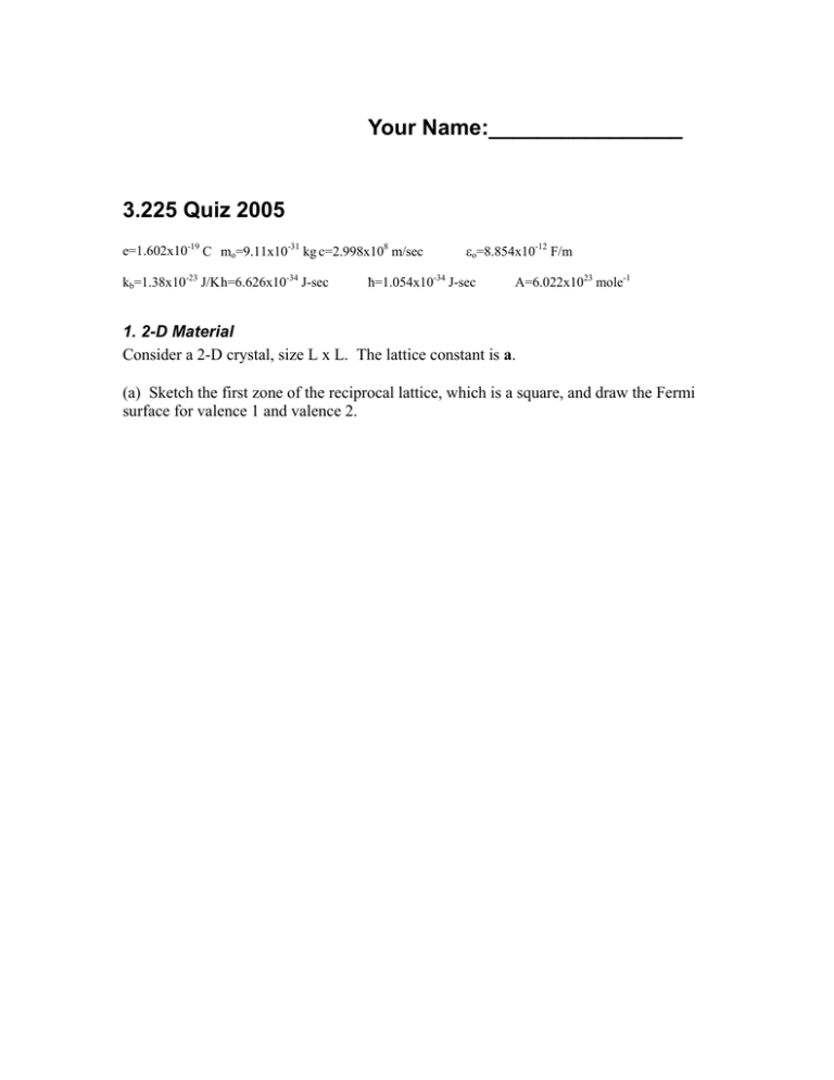
Your Name:________________ 3.225 Quiz 2005 e=1.602x10⁻¹⁹ C mo=9.11x10⁻³¹ kg c=2.998x10⁸ m/sec kb=1.38x10⁻²³ J/Kh=6.626x10-34 J-sec εo=8.854x10⁻¹² F/m ħ=1.054x10⁻³⁴ J-sec A=6.022x10²³ mole-1 1. 2-D Material Consider a 2-D crystal, size L x L. The lattice constant is a. (a) Sketch the first zone of the reciprocal lattice, which is a square, and draw the Fermi surface for valence 1 and valence 2. (b) Now draw a separate sketch of E vs. k along the [10] and [11] directions. Sketch only the first and second bands. Indicate kF and EF, for valence (Z) equal to 1 and valence equal 2 cases. Assume U is about 25% of the EF(Z=1). (c) Describe the expected conductivity in Z=1 and Z=2 material at room temperature and T=0 K. (d) When the size of the crystal shrinks to L=8a, derive an equation (for a general valence Z) that defines the set of points on the Fermi surface that remain valid conducting states in the new smaller material. 2. Free electron model in aluminum (a) Determine the conductivity, scattering length, and reflection spectra (reflection vs. wavelength) of Al using the Drude/free electron model assuming a scattering time of 10 14 seconds. Al is valence 3. (b) How does the scattering length compare with inter-atomic distance? What dislocation density would be needed to decrease the conductivity by a factor of 10? What effective size of dislocation would be necessary to achieve this density? Is this possible? (c) Determine the conductivity of Si (atomic number 14) using the Drude model and compare it to the value you expect for Al. Does this value match experiment? Explain. 3. Steering Photons Methods of switching propagating directions of photons are an active area of research, since optical switching in the network is a desirable attribute. One way to do this is to change the carrier concentration in a semiconductor through an applied potential. The index of refraction is a function of the free carrier concentration, and therefore the index can be changed through application of an electrical potential. This can lead to photon switching in optimized device geometry. A simplified concept of this device is simply a p-n junction, shown schematically below. hν Metallurgical junction n+=1020 cm-3 p=NA cm-3 X1 X0 Note this is a n+-p junction. Without reverse bias, the depletion region on the p-side is labeled X0, whereas when a reverse bias VR is applied, it becomes X1. Light is entering as shown by the arrow. A. Describe how this device can affect the propagation of the light in the material by introducing an index change. B. Assume that we need at least one micron between X0 and X1 in order to have the light propagate sufficiently. For a given reverse bias VA, determine an expression that relates NA to VR. 4. Dielectrics Describe why non-conducting materials have an index of refraction that is greater than the value 1, and also why such materials tend to be transparent. For such a material, describe the expected frequency dependence of the dielectric constant.
