MASSACHUSETTS INSTITUTE OF TECHNOLOGY 6.071 Introduction to Electronics, Signals and Measurement
advertisement
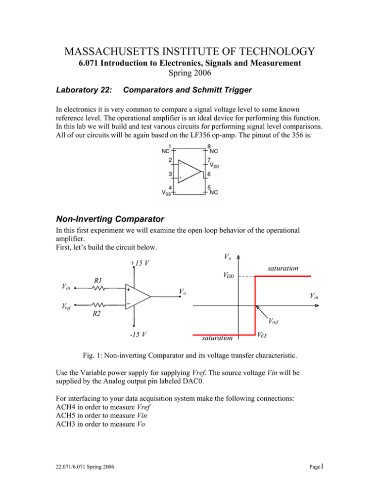
MASSACHUSETTS INSTITUTE OF TECHNOLOGY 6.071 Introduction to Electronics, Signals and Measurement Spring 2006 Laboratory 22: Comparators and Schmitt Trigger In electronics it is very common to compare a signal voltage level to some known reference level. The operational amplifier is an ideal device for performing this function. In this lab we will build and test various circuits for performing signal level comparisons. All of our circuits will be again based on the LF356 op-amp. The pinout of the 356 is: Non-Inverting Comparator In this first experiment we will examine the open loop behavior of the operational amplifier. First, let’s build the circuit below. Vo +15 V saturation VDD R1 Vin Vo Vin Vref R2 Vref -15 V saturation VEE Fig. 1: Non-inverting Comparator and its voltage transfer characteristic. Use the Variable power supply for supplying Vref. The source voltage Vin will be supplied by the Analog output pin labeled DAC0. For interfacing to your data acquisition system make the following connections: ACH4 in order to measure Vref ACH5 in order to measure Vin ACH3 in order to measure Vo 22.071/6.071 Spring 2006 Page1 Use the +15V and the -15V DC to power your amplifier. Before proceeding with the experiment answer the following questions: How is Vo related to Vin and Vref? Why is this circuit called a non-inverting comparator? What do you think is the role of resistors R1 and R2? Next let’s run the experiment and observe the behavior of this circuit. Download the virtual instrument called Comparator from the class web site. Note that you will provide Vref from the Variable Power Supply of your system while Vin is provided by the Analog Output pin labeled DAC0. The instrument looks like: Courtesy of National Instruments. Used with permission. 22.071/6.071 Spring 2006 Page2 Set Vref = 0 Volts and for Vin use a sign wave with an amplitude of 3 V and frequency of 20Hz. Observe the output Vo. Draw the form of Vo on the graph below. Indicate the maximum and minimum values for Vo on the graph. What do these maximum and minimum values correspond to? Now change Vref to +1V. What is the output in this case? Draw the output on the graph below. Now lets use our comparator to adjust the duty-cycle of the square wave out put (the voltage Vo). From your experiment determine the value of Vref that results in a square 22.071/6.071 Spring 2006 Page3 wave output with a duty-cycle of 20% . If you wanted a duty cycle of 80% what would you do? In addition to the non-inverting comparator, the open loop characteristics of the op-amp may also be exploited in the inverting comparator configuration. A typical inverting comparator circuit is shown below. +15 V Vref R1 Vo Vin R2 -15 V For this inverting case draw the response of the circuit on the graph below. (The thick horizontal solid line represents Vref.) 22.071/6.071 Spring 2006 Page4 Comparator and noise. Next we will look at the response of the comparator in the presence of noise. The circuit is still the same non-inverting comparator as the one shown on Fig. 1., reproduced here for convenience. +15 V Vin R1 Vo Vref R2 -15 V Now the signal Vin has some form of noise associated with it and it might look like the one represented by the jagged line shown on Fig. 3. A closer look at the signal shows that there are multiple times, within 1 cycle, that it goes above and below 1 Volt, the reference voltage in this case. Each of these transitions will be detected by the comparator and will be represented as a transition at the output. For the example below draw the expected form for the output. Figure 3. A signal with noise and a reference voltage. Your Comparator virtual instrument is designed to provide a signal with simulated noise for the purpose of this laboratory. You can introduce the “noise” into your input signal by entering the desired noise amplitude. 22.071/6.071 Spring 2006 Page5 Once you have generated your “noisy” signal the response of the comparator will look something like: Notice the transitions resulting from the signal noise. Vary the reference voltage Vref and observe the response of the circuit. What happens when Vref becomes greater than the maximum value of Vin? What happens when Vref becomes less than the minimum value of Vin? If your application required the detection of a signal transition above or below a certain value the open-loop comparator circuit would be a useful as long as the signal is completely free of any noise. In the presence of noise, which is the case in all practical situations, the comparator exhibits unacceptable behavior. The solution to this problem is provided by positive feedback. 22.071/6.071 Spring 2006 Page6 Schmitt Trigger. Positive Feedback The Schmitt Trigger circuit, also called a bistable multivibrator, uses positive feedback with loop gain greater than 1 to produce a bistable (High – Low) response. The Schmitt trigger may be designed to be inverting or non-inverting. These two circuits with their corresponding characteristics are shown below. Non-inverting Schmitt Trigger Vo VH Rp V- Vref VTU Vin VTL Vo VS V+ Vin R1 VL R2 ⎛ R VS = ⎜1 + 1 ⎝ R2 ⎞ R1 R , VTL = VS − VH 1 ⎟ Vref , VTU = VS − VL R2 R2 ⎠ Inverting Schmitt Trigger Vo VH Rp Vin Vref V- VTU Vin VTL Vo VS V+ R1 VL R2 VS = Vref R2 R1 R1 , VTU = VS + VH , VTL = VS + VL R1 + R2 R1 + R2 R1 + R2 22.071/6.071 Spring 2006 Page7 For our experiment we will work with the inverting Schmitt Trigger configuration. Construct the following circuit on your protoboard. Note that this may be accomplished with minor changes to your open loop comparator circuit used before. Rp Vin Vref V- Vo V+ R1 R2 Again the connections to your protoboard are the same as the comparator case. ACH4 measures Vref ACH5 measures Vin ACH3 measures Vo Now download the virtual instrument called Inv_S_Trigger from the class web site. It will look like: Courtesy of National Instruments. Used with permission. 22.071/6.071 Spring 2006 Page8 This instrument is constructed in order to give you the opportunity to experiment with all parameters that characterize the behavior of the trigger circuit. The width of the hysteresis loop determines the noise immunity of the trigger circuit. The position and width of the hysteresis may be designed for the problem of interest. Have some fun, vary the circuit parameters and the signal characteristics and observe the output. With R1=1k and R2=10k, run the experiment with a clean signal (no noise) and with Vref=1Volt. You might also need to adjust the amplitude and the offset of input signal Vin. Observe the behavior of the circuit and determine Vs, VTU and VTL. Compare with measurement. Do you see any differences? 22.071/6.071 Spring 2006 Page9

