Document 13383755
advertisement
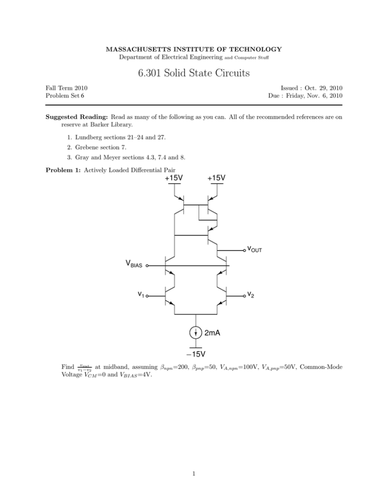
MASSACHUSETTS INSTITUTE OF TECHNOLOGY Department of Electrical Engineering and Computer Stuff 6.301 Solid State Circuits Fall Term 2010 Problem Set 6 Issued : Oct. 29, 2010 Due : Friday, Nov. 6, 2010 Suggested Reading: Read as many of the following as you can. All of the recommended references are on reserve at Barker Library. 1. Lundberg sections 21–24 and 27. 2. Grebene section 7. 3. Gray and Meyer sections 4.3, 7.4 and 8. Problem 1: Actively Loaded Differential Pair +15V +15V vOUT VBIAS v1 v2 2mA _ 15V Find vv1out −v2 at midband, assuming βnpn =200, βpnp =50, VA,npn =100V, VA,pnp =50V, Common-Mode Voltage VCM =0 and VBIAS =4V. 1 Problem 2: Op Amp Log Circuit Assume that the following circuit is operated at room temperature (T = 300K). iR − + 1k − R1 iIN + vO _ + R2 (a) When R1 =15.7R2 , vO is of the form vO =A log10 (x). Find A and x. (b) Solve for R1 in terms of R2 such that vO exhibits a log2 (x) behavior. Problem 3: Op Amp Frequency Response Assume that the following op amp has a finite gain with frequency ao response A(s)= τ s+1 (where ao =106 and τ =10−6 ) and that f =[1 0.1 0.01 0.001]. + vIN vOUT A(s) − (1-ƒ)R ƒR (a) Solve for the closed-loop DC gain and upper −3dB Frequency for each value of f . (b) Sketch the Bode plot (magnitude only) of vOU T vIN (s) for each value of f . (c) Sketch the unit step response of vOUT (t) for each value of f . Make sure to label important features in your sketches including magnitudes, slopes, breakpoint frequencies, and times. Problem 4: Lead-Lag Op Amp Configuration 10k 100k 10uF vIN − 1k 1nF vOUT + T Sketch the Bode plot (magnitude and phase) of vvOU (s). Make sure to label the magnitudes of each IN asymptote and its breakpoint frequency. Assume the op amp is ideal. 2 MIT OpenCourseWare http://ocw.mit.edu 6.301 Solid-State Circuits Fall 2010 For information about citing these materials or our Terms of Use, visit: http://ocw.mit.edu/terms.
