in situ transistors
advertisement

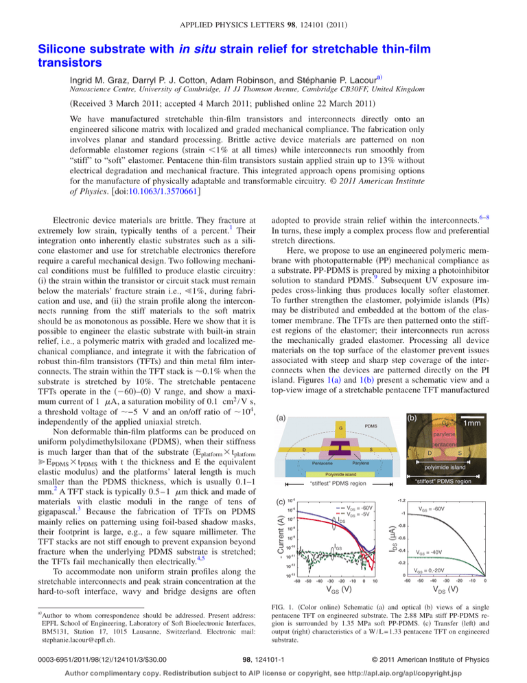
APPLIED PHYSICS LETTERS 98, 124101 共2011兲 Silicone substrate with in situ strain relief for stretchable thin-film transistors Ingrid M. Graz, Darryl P. J. Cotton, Adam Robinson, and Stéphanie P. Lacoura兲 Nanoscience Centre, University of Cambridge, 11 JJ Thomson Avenue, Cambridge CB30FF, United Kingdom 共Received 3 March 2011; accepted 4 March 2011; published online 22 March 2011兲 We have manufactured stretchable thin-film transistors and interconnects directly onto an engineered silicone matrix with localized and graded mechanical compliance. The fabrication only involves planar and standard processing. Brittle active device materials are patterned on non deformable elastomer regions 共strain ⬍1% at all times兲 while interconnects run smoothly from “stiff” to “soft” elastomer. Pentacene thin-film transistors sustain applied strain up to 13% without electrical degradation and mechanical fracture. This integrated approach opens promising options for the manufacture of physically adaptable and transformable circuitry. © 2011 American Institute of Physics. 关doi:10.1063/1.3570661兴 a兲 Author to whom correspondence should be addressed. Present address: EPFL School of Engineering, Laboratory of Soft Bioelectronic Interfaces, BM5131, Station 17, 1015 Lausanne, Switzerland. Electronic mail: stephanie.lacour@epfl.ch. 0003-6951/2011/98共12兲/124101/3/$30.00 adopted to provide strain relief within the interconnects.6–8 In turns, these imply a complex process flow and preferential stretch directions. Here, we propose to use an engineered polymeric membrane with photopatternable 共PP兲 mechanical compliance as a substrate. PP-PDMS is prepared by mixing a photoinhibitor solution to standard PDMS.9 Subsequent UV exposure impedes cross-linking thus produces locally softer elastomer. To further strengthen the elastomer, polyimide islands 共PIs兲 may be distributed and embedded at the bottom of the elastomer membrane. The TFTs are then patterned onto the stiffest regions of the elastomer; their interconnects run across the mechanically graded elastomer. Processing all device materials on the top surface of the elastomer prevent issues associated with steep and sharp step coverage of the interconnects when the devices are patterned directly on the PI island. Figures 1共a兲 and 1共b兲 present a schematic view and a top-view image of a stretchable pentacene TFT manufactured (a) (b) 1mm G parylene pentacene D S polyimide island “stiffest” PDMS region “stiffest” PDMS region -5 -1.2 10-6 10-7 IDS VDS = -60V VDS = -5V -1 IDS (A) (c) 10 - Current (A) Electronic device materials are brittle. They fracture at extremely low strain, typically tenths of a percent.1 Their integration onto inherently elastic substrates such as a silicone elastomer and use for stretchable electronics therefore require a careful mechanical design. Two following mechanical conditions must be fulfilled to produce elastic circuitry: 共i兲 the strain within the transistor or circuit stack must remain below the materials’ fracture strain i.e., Ⰶ1%, during fabrication and use, and 共ii兲 the strain profile along the interconnects running from the stiff materials to the soft matrix should be as monotonous as possible. Here we show that it is possible to engineer the elastic substrate with built-in strain relief, i.e., a polymeric matrix with graded and localized mechanical compliance, and integrate it with the fabrication of robust thin-film transistors 共TFTs兲 and thin metal film interconnects. The strain within the TFT stack is ⬃0.1% when the substrate is stretched by 10%. The stretchable pentacene TFTs operate in the 共⫺60兲–共0兲 V range, and show a maximum current of 1 A, a saturation mobility of 0.1 cm2 / V s, a threshold voltage of ⬃−5 V and an on/off ratio of ⬃104, independently of the applied uniaxial stretch. Non deformable thin-film platforms can be produced on uniform polydimethylsiloxane 共PDMS兲, when their stiffness is much larger than that of the substrate 共Eplatform ⫻ tplatform Ⰷ EPDMS ⫻ tPDMS with t the thickness and E the equivalent elastic modulus兲 and the platforms’ lateral length is much smaller than the PDMS thickness, which is usually 0.1–1 mm.2 A TFT stack is typically 0.5– 1 m thick and made of materials with elastic moduli in the range of tens of gigapascal.3 Because the fabrication of TFTs on PDMS mainly relies on patterning using foil-based shadow masks, their footprint is large, e.g., a few square millimeter. The TFT stacks are not stiff enough to prevent expansion beyond fracture when the underlying PDMS substrate is stretched; the TFTs fail mechanically then electrically.4,5 To accommodate non uniform strain profiles along the stretchable interconnects and peak strain concentration at the hard-to-soft interface, wavy and bridge designs are often 10-8 10-9 IGS 10-10 -0.8 -0.6 -0.4 10-11 VGS = -40V -0.2 10-12 10-13 -60 VGS = -60V -50 -40 -30 -20 -10 VGS (V) 0 10 0 -60 VGS = 0,-20V -50 -40 -30 -20 -10 0 VDS (V) FIG. 1. 共Color online兲 Schematic 共a兲 and optical 共b兲 views of a single pentacene TFT on engineered substrate. The 2.88 MPa stiff PP-PDMS region is surrounded by 1.35 MPa soft PP-PDMS. 共c兲 Transfer 共left兲 and output 共right兲 characteristics of a W / L = 1.33 pentacene TFT on engineered substrate. 98, 124101-1 © 2011 American Institute of Physics Author complimentary copy. Redistribution subject to AIP license or copyright, see http://apl.aip.org/apl/copyright.jsp Appl. Phys. Lett. 98, 124101 共2011兲 Graz et al. -6 (a) 10 VDS = -60V VDS = -5V εappl = 12.6% -1 IDS 10-8 10 IGS 10-10 0.12 (a) εappl = 12.6% VGS = -60V -0.8 -9 -0.6 -0.4 10-11 relaxed VGS = -40V -0.2 -40 -30 -20 VGS (V) -10 0 10 0 -60 -50 -40 0.1 0.09 0.08 0.07 -20 -10 0 FIG. 2. 共Color online兲 Transfer 共left兲 and output 共right兲 characteristics of a W / L = 1.33 pentacene TFT on engineered substrate held stretched at 12.7% strain. on such substrate. The fabrication process starts with the definition of PI islands 共2 mm in diameter, 50 m thick, 6 mm apart兲 on a silicon wafer coated with a water-soluble release layer. The wafer is then coated with a ⬃100 m thick PP-PDMS layer. PP-PDMS preparation is described in details in Ref. 9. PP-PDMS is UV-exposed through a positive mask 共UV dose= 1.2 J cm−2兲 to define “stiff” 2.4 mm diameter regions concentric with the PI islands. The equivalent elastic moduli 共based on the Money–Rivlin model of the elastomer兲 of the non exposed and UV irradiated PP-PDMS are 2.88 MPa and 1.35 MPa, respectively.9 The engineered polymeric membrane is then cured for 24 h at 150 ° C in an air oven. To simplify the final peeling process, the graded substrate is mounted on a plastic foil 共Kapton HN, Dupont兲 and the bottom gate staggered organic TFT process begins. The TFT stack consists of a thermally evaporated, 5 nm/30 nm thick chromium/gold 共Cr/Au兲 bilayer 共gate electrode兲, a 600 nm thick poly-para-xylylene 共parylene C, Labcoater 2010, Specialty Coating Systems兲 dielectric layer, and a thermally evaporated 50 nm thick pentacene film 共98% purity, Sigma, Aldrich兲. A 30 nm thick gold film for the source and drain contacts completes the TFTs. Each thin film is patterned using a shadow mask and aligned by eye. The electromechanical characterization of the devices is conducted in a N2 environment glovebox fitted with a manual stretcher. The TFTs 共W / L = 200 m / 100 m兲 on engineered substrate are peeled off their Kapton backing 共bending radius ⬃2 mm兲 then mounted free-standing in the stretcher. The device films are crack-free 关Fig. 1共b兲兴, which is a key condition for their electrical functionality. Standard probes contact the gold pads on PDMS via a compliant silver polymer dag 共ESL1901-s, Electroscience Laboratories兲. The transfer and output characteristics of a pentacene TFT on engineered substrate are presented in Fig. 1共c兲. No strain is applied to the device. The TFT operates in the 共⫺60兲–共0兲 V range. The saturation mobility sat is 0.105 cm2 / V s, the on-off ratio is 8.6⫻ 103, and the threshold voltage Vt is ⫺5 V. The device has a low leakage gate current of 6 ⫻ 10−11 A. This performance is comparable to that reported from pentacene TFTs on PDMS 共Ref. 5兲 and flexible substrates.10 Figure 2 summarizes the I共V兲 curves of the pentacene TFT held at 12.6% strain. The TFT response is little affected by the large mechanical deformation with sat = 0.106 cm2 / V s and Vt = −4 V. The small hysteresis observed in the output curves is attributed to the electrical contact between the polymer Ag dag and the tungsten probes, which need to be lifted up and repositioned at each strain. relaxed, after 2 days in air 0.06 0.05 -30 VDS (V) (b) 0.11 stretched -2 0 2 4 6 8 10 12 14 Applied tensile strain (%) -4 (c) (d) 1.4 VDS = -60V -6 1.2 relaxed, after 2 days in air -8 I/I0 -50 VGS = 0,-20V Vt (V) 10-12 10-13 -60 (b) -1.2 IDS (A) - Current (A) 10-7 Mobility (cm2/V.s) 124101-2 1 -10 0.8 -12 relaxed, after 2 days in air 0.6 -14 -2 0 2 4 6 8 10 12 14 Applied tensile strain (%) -2 0 2 4 6 8 10 12 14 Applied tensile strain (%) FIG. 3. 共Color online兲 共a兲 Optical views of stretchable TFTs on engineered substrate. 共b兲 Saturation mobility, threshold voltage and channel on current as a function of applied mechanical strain. Figure 3共a兲 illustrates a membrane with six TFTs uniaxially stretched. The longitudinal extension of the Au interconnects in-between the TFTs is clearly visible. Figures 3共b兲–3共d兲 summarizes the TFT response with strain. Negligible changes in mobility, Vt and output current of the device are observed. Stretching further 共⬎13%兲 often results in delamination of the polymer Ag dag from the soft substrate. After release, the TFTs are not probed but kept for two days in air. Under the optical microscope, the device films appear smooth and crack-free after the mechanical stretching cycle indicating that the strain within the TFT stack did not exceed their fracture strain. After two days in air, the TFTs remain functional but their electrical performance has degraded. This is attributed to the oxidation of the pentacene rather than mechanical damage to the TFT channels. To quantify the strain levels and distribution within the engineered substrate, we simulate the deformation of the substrate under 10% tensile applied strain using threedimensional finite element modeling 共Comsol兲. The elastomer is simulated with the hyperelastic Mooney–Rivlin model and fitted parameters from experimental stress-strain curves.9,11 The 730 nm thick TFT stack is not modeled. The engineered substrate is 100 m thick; the PI island is 50 m thick, 2 mm diameter. Figures 4共a兲 and 4共b兲 show two strain color plots of the substrate with a PI island embedded in a uniform and 2-moduli PP-PDMS, and strain profiles at the top surface of the engineered substrates, top. A uniform PDMS substrate expands uniformly, the strain across the whole substrate equals the applied strain 共data not shown兲. When a PI island is embedded at the bottom of a uniform PDMS substrate, top is pinned to 0.1% in the region immediately above the PI island then increases to top,max ⬃ 18.1%, a few hundreds of micrometer beyond the island edge 共profile A-A, Fig. 4兲 and decreases to 10% strain away from the island. The diameter of the ⬃0% region aligned with the PI island is 1.1mm. Using a 2-moduli PP-PDMS with its stiffest region centered on the PI island allows for Author complimentary copy. Redistribution subject to AIP license or copyright, see http://apl.aip.org/apl/copyright.jsp 124101-3 first principal strain (%) A A B B strain at top surface (%) (a) 20 Appl. Phys. Lett. 98, 124101 共2011兲 Graz et al. (b) 15 10 5 0 A-A B-B 5 moduli 0 0.5 1 1.5 2 2.5 position (mm) 3 6 (c) 5 4 3 2 1 0 0 0.2 0.4 0.6 0.8 1 substrate thickness (mm) FIG. 4. 共Color online兲 Finite element modeling of engineered substrates with built-in strain relief. 共a兲 First principal strain color cross-sections of substrates prepared with 共top兲 a uniform PP-PDMS membrane 共1.35 MPa兲, and 共bottom兲 a 2-moduli PP-PDMS membrane 共2.88 MPa; 2.4 mm diameter and 1.35 MPa matrix兲. The x-axis runs along the radius of the 50 m thick PI island and starts at its center 共x = 0兲. 共b兲 Strain profiles at the top surface of the elastomer for three types of substrates: Uniform, 2-moduli, and 5 moduli PP-PDMS membranes. The 5-moduli substrate is designed with concentric PP-PDMS rings of 2.88 MPa; 2.4 mm diameter, 1.8 MPa; 2.8 mm diameter, 1.35 MPa; 3.2 mm diameter, 0.96 MPa; 3.6 mm diameter, and 0.65 MPa for the matrix. 共c兲 Strain at the center of the stiff elastomer surface 共x = 0兲 as a function of the thickness of the PP-PDMS membrane. 0% strain of the top elastomer surface depends on the PI island to elastomer thickness ratio, R. Figure 4共c兲 plots top at x = 0 mm i.e., above the center of the PI island, as a function of the elastomer thickness for a 50 m thick PI island. The applied strain is 10%. top increases quickly to values above 1% when the substrate is thicker than 200 m. This suggests R should be at least 0.25. In summary, we have demonstrated that stretchable thinfilm transistors can be fabricated directly onto elastomeric substrates. The proposed strain relief method based on photopatterned graded stiffness of the elastomer combined with embedded plastic islands is efficient to ensure TFT materials are not stretched above their fracture strains 共⬍1%兲, and can be tuned to develop a low strain profile across the elastic thin film interconnects running in-between the nondeformable elastomeric regions. Furthermore this method is not limited to organic TFTs and should be easily transferred to other thin-film devices including low temperature amorphous silicon and zinc oxide TFTs. The direct integration of microelectronic devices onto engineered elastomeric substrates has the potential to influence the design of most existing stretchable circuits and therefore, opens up a wide range of exciting opportunities. This research is supported by the Royal Society, the collaboration between the University of Cambridge and Nokia, and the EPSRC 共EP/G020930/1兲. We would like to thank Prof. H. Sirringhaus for providing access to the electrical characterization glovebox. 1 the widening of the no-deformation region at the top surface 共profile B-B, Fig. 4兲. Using a 2.4 mm diameter, 2.88 MPa stiff PP-PDMS volume surrounded by 1.35 MPa soft PPPDMS allows for a 1.6 mm diameter undeformable region above the PI island. Note that the striking color transition at x = 1.2 mm comes from the discrete boundaries between the two elastomers of different modulus. Further simulations show that using more steps in the compliance gradient 关a 5-moduli elastomer is used Fig. 4共b兲兴 further widens the ⬃0% region at the surface of the elastomer 共to 1.7 mm diameter兲 but more importantly the strain increase across the stiff-to-soft interface may be greatly reduced 共from 48%/mm with no grading down to 15%/mm with 5-moduli兲. This could be achieved by exposing the PP-PDMS membrane with five successive UV exposures through five concentric positive masks or in a single exposure using a graded binary mask 共experiments not done兲. Finally the pinning to nearly Z. Suo, Encyclopedia of Materials: Science and Technology, Second edition, 共Elsevier, Oxford, 2003兲, pp. 3290–3296. 2 S. P. Lacour, S. Wagner, R. Narayan, T. Li, and Z. Suo, J. Appl. Phys. 100, 014913 共2006兲. 3 S. Wagner, H. Gleskova, I.-C. Cheng, J. C. Sturm, and Z. Suo, in Flexible Flat Panel Displays, edited by G. P. Crawford 共Wiley, New York, 2005兲, pp. 263–283. 4 S. P. Lacour and S. Wagner, Tech. Dig. - Int. Electron Devices Meet. 2005, 5.2.1. 5 I. Graz and S. P. Lacour, Appl. Phys. Lett. 95, 243305 共2009兲. 6 D. Brosteaux, F. Axisa, M. Gonzalez, and J. Vanfleteren, IEEE Electron Device Lett. 28, 552 共2007兲. 7 J. A. Rogers, T. Someya, and Y. Huang, Science 327, 1603 共2010兲. 8 J. Lee, J. W. M. Shi, J. Yoon, S.-I. Park, M. Li, Z. Liu, Y. Huang, and J. A. Rogers, Adv. Mater. 23, 986 共2011兲. 9 D. P. J. Cotton, A. Popel, I. M. Graz, and S. P. Lacour, J. Appl. Phys. 109, 054905 共2011兲. 10 L. Zhou, A. Wanga, S.-C. Wu, J. Sun, S. Park, and T. N. Jackson, Appl. Phys. Lett. 88, 083502 共2006兲. 11 A. N. Gent, Engineering with Rubber: How to Design Rubber Components, 2nd ed. 共Hanser Gardner, Cincinnati, 2001兲. Author complimentary copy. Redistribution subject to AIP license or copyright, see http://apl.aip.org/apl/copyright.jsp


