Terminating Surface Electromigration at the Source Kirk H. Bevan, Wenguang Zhu, Hong Guo,
advertisement
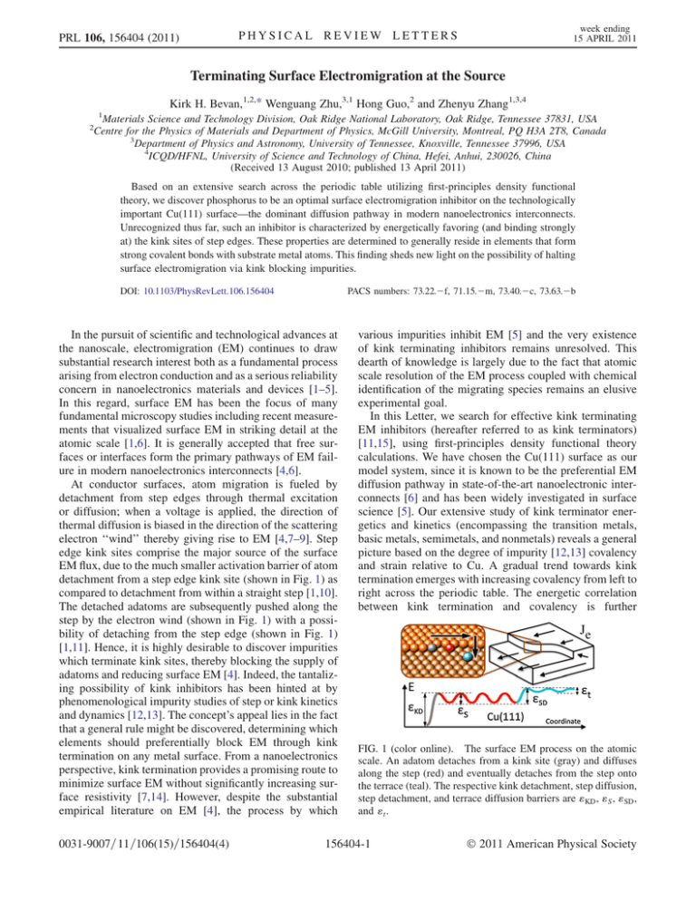
PRL 106, 156404 (2011) week ending 15 APRIL 2011 PHYSICAL REVIEW LETTERS Terminating Surface Electromigration at the Source Kirk H. Bevan,1,2,* Wenguang Zhu,3,1 Hong Guo,2 and Zhenyu Zhang1,3,4 1 Materials Science and Technology Division, Oak Ridge National Laboratory, Oak Ridge, Tennessee 37831, USA Centre for the Physics of Materials and Department of Physics, McGill University, Montreal, PQ H3A 2T8, Canada 3 Department of Physics and Astronomy, University of Tennessee, Knoxville, Tennessee 37996, USA 4 ICQD/HFNL, University of Science and Technology of China, Hefei, Anhui, 230026, China (Received 13 August 2010; published 13 April 2011) 2 Based on an extensive search across the periodic table utilizing first-principles density functional theory, we discover phosphorus to be an optimal surface electromigration inhibitor on the technologically important Cu(111) surface—the dominant diffusion pathway in modern nanoelectronics interconnects. Unrecognized thus far, such an inhibitor is characterized by energetically favoring (and binding strongly at) the kink sites of step edges. These properties are determined to generally reside in elements that form strong covalent bonds with substrate metal atoms. This finding sheds new light on the possibility of halting surface electromigration via kink blocking impurities. DOI: 10.1103/PhysRevLett.106.156404 PACS numbers: 73.22.f, 71.15.m, 73.40.c, 73.63.b In the pursuit of scientific and technological advances at the nanoscale, electromigration (EM) continues to draw substantial research interest both as a fundamental process arising from electron conduction and as a serious reliability concern in nanoelectronics materials and devices [1–5]. In this regard, surface EM has been the focus of many fundamental microscopy studies including recent measurements that visualized surface EM in striking detail at the atomic scale [1,6]. It is generally accepted that free surfaces or interfaces form the primary pathways of EM failure in modern nanoelectronics interconnects [4,6]. At conductor surfaces, atom migration is fueled by detachment from step edges through thermal excitation or diffusion; when a voltage is applied, the direction of thermal diffusion is biased in the direction of the scattering electron ‘‘wind’’ thereby giving rise to EM [4,7–9]. Step edge kink sites comprise the major source of the surface EM flux, due to the much smaller activation barrier of atom detachment from a step edge kink site (shown in Fig. 1) as compared to detachment from within a straight step [1,10]. The detached adatoms are subsequently pushed along the step by the electron wind (shown in Fig. 1) with a possibility of detaching from the step edge (shown in Fig. 1) [1,11]. Hence, it is highly desirable to discover impurities which terminate kink sites, thereby blocking the supply of adatoms and reducing surface EM [4]. Indeed, the tantalizing possibility of kink inhibitors has been hinted at by phenomenological impurity studies of step or kink kinetics and dynamics [12,13]. The concept’s appeal lies in the fact that a general rule might be discovered, determining which elements should preferentially block EM through kink termination on any metal surface. From a nanoelectronics perspective, kink termination provides a promising route to minimize surface EM without significantly increasing surface resistivity [7,14]. However, despite the substantial empirical literature on EM [4], the process by which 0031-9007=11=106(15)=156404(4) various impurities inhibit EM [5] and the very existence of kink terminating inhibitors remains unresolved. This dearth of knowledge is largely due to the fact that atomic scale resolution of the EM process coupled with chemical identification of the migrating species remains an elusive experimental goal. In this Letter, we search for effective kink terminating EM inhibitors (hereafter referred to as kink terminators) [11,15], using first-principles density functional theory calculations. We have chosen the Cu(111) surface as our model system, since it is known to be the preferential EM diffusion pathway in state-of-the-art nanoelectronic interconnects [6] and has been widely investigated in surface science [5]. Our extensive study of kink terminator energetics and kinetics (encompassing the transition metals, basic metals, semimetals, and nonmetals) reveals a general picture based on the degree of impurity [12,13] covalency and strain relative to Cu. A gradual trend towards kink termination emerges with increasing covalency from left to right across the periodic table. The energetic correlation between kink termination and covalency is further FIG. 1 (color online). The surface EM process on the atomic scale. An adatom detaches from a kink site (gray) and diffuses along the step (red) and eventually detaches from the step onto the terrace (teal). The respective kink detachment, step diffusion, step detachment, and terrace diffusion barriers are "KD , "S , "SD , and "t . 156404-1 Ó 2011 American Physical Society PRL 106, 156404 (2011) PHYSICAL REVIEW LETTERS strengthened by kinetic barrier results, which yield a clear preference for semimetal and nonmetal terminators that can be understood by contrasting metallic and covalent bonding [16]. We predict P to be the optimal Cu(111) kink terminator element. Our first-principles density functional theory calculations were performed using the VASP code [17], with electron-ion interactions represented within the projector augmented wave (PAW) approach [18] and electron exchange-correlation modeled within the generalized gradient approximation (Perdew-Burke-Ernzerhof GGA) [19]. The default VASP-PAW potential database Cu planewave cutoff energy of 273.214 eV was applied in all calculations; where necessary, for very light impurity elements, the cutoff energy was increased to up to 400.00 eV. To aid convergence, the Fermi-level smearing approach of Methfessel and Paxton [20] was employed at a Gaussian width of 0.1 eV. Optimized atomic geometries were achieved when forces on all unconstrained atoms were The Cu bulk smaller in magnitude than 0:01 eV=A. 3.64 Å lattice constant obtained by this approach matches well with the experimental value of 3.63 Å [11]. Transition state diffusion pathways were determined by way of the ‘‘climbing image nudged elastic band’’ method [21], whereafter spline interpolation was applied to determine kinetic energy barriers. To study the EM trends of kink atoms on the Cu(111) surface, we used 5-layer (854) and (874) miscut slabs with a total of 65 and 74 atoms to model the kinks at the edges of f100g and f111g mini-faceted steps, respectively [15]. Both slabs possess h110i oriented steps interrupted by a kink every fourth atom and separated by (111) terraces four atomic rows wide. In the calculations, the bottom two layers were frozen at their bulk coordinates and the Brillouin zone was sampled at 5 5 1 reciprocal points [22]. To eliminate interactions between supercell images, each slab was separated by a 11.5 Å vacuum region. All of the results presented here where obtained on the Cu(854) miscut surface, calculations were repeated on the Cu(874) miscut surface for those impurity elements which were found to function as kink terminators on Cu(854)—the two miscut results exhibited the same trends. To inhibit EM through kink termination, an impurity must meet two fundamental criteria: first, energetically favor bonding at a kink site (rather than attaching to a step, sitting on a terrace, or embedding into a step); second, possess a kink detachment barrier "KD which exceeds that of the conductor material (see Fig. 1). In the remainder of this Letter we examine which elements across the periodic table are most likely to satisfy these kink terminator criteria. We first investigate the energetic preference that impurity adatoms have for attachment at a kink [site A in Fig. 2(a)], attachment at a step [site B in Fig. 2(a)], and embedding into a step [sites C, D, and E in Fig. 2(a)]. week ending 15 APRIL 2011 FIG. 2 (color online). Total energies for step impurities juxtaposed against kink barriers on Cu(854). (a) Total energies for kink attachment (solid gray squares), step attachment (dotted red circles), and three step embedding configurations (dashed blue open triangles, dot-dashed green open diamonds, and doubledot-dashed purple crosses). (b) Barriers for detachment from the kink site to the step edge "KD (solid grad squares) and attachment to the kink from the step "S (dotted red circles). Elements commonly used to prevent Cu EM are labeled in bold [23]. Periodic table group assignments are given. The total energy for each of these configurations on the Cu(854) miscut surface, relative to the reference energy for kink termination, is shown in Fig. 2(a) for a wide range of impurity adatoms. Those elements which have been empirically reported to inhibit Cu EM are labeled in bold [4,23]. Various energetic trends emerge upon examination of the results presented in Fig. 2(a). Consider first the transition metals to the left of Cu in the periodic table which, having a less filled shell relative to Cu, favor gaining electrons by accumulating bonding neighbors and therefore tend to embed into Cu(111) steps. whereas transition metals to the right of Cu have a more filled valance shell and favor attachment at a kink site [11]. As we move into the p-block elements, the basic metals are tempered by both their atomic radii and shell valance. Those with large atomic radii relative to Cu, namely, In, Tl, Sn, Pb, and Bi, introduce strain into the step or terrace and therefore prefer to sit at a kink site. Those with smaller atomic radii, namely, Al and Ga, lack any energetic cost due to strain and prefer to gain bonding neighbors by embedding into a step. In addition, it has been reported that several of the larger basic metals including Sn, Sb, In, Pb, and Bi embed or alloy into Cu(111) terraces [24] and may inhibit EM by roughing terraces [5]—this important mechanism [5] is not negated by the results presented in this Letter. Note that covalency begins to appear in the semimetals, which generally favor kink termination due to the 3 Cu bonding neighbors present at kink sites [16]—in this regard, Si=Ge, Sb=As, and Te have an unfilled shell of 4, 3, and 2, respectively. The nonmetals altogether avoid embedding into step edges and only the largest nonmetals (P, S, and Se) prefer kink sites. The p-block halogen elements, namely, Cl, Br, and I, absent from Fig. 2 have all been found to prefer either step edge or terrace attachment by approximately 0.1–0.2 eV. The smaller p-block elements 156404-2 PRL 106, 156404 (2011) PHYSICAL REVIEW LETTERS B, C, N, O, and F have been excluded from this study due to their small atomic radii relative to Cu. They were usually found to either diffuse into the surface or bind in a complex manner not consistent with the normal adatom diffusion picture (see Fig. 1). Overall, basic metals having a large atomic radius and nonmetals, where 2 or 3 electrons are required to fill the valance shell, are energetically the best EM kink terminator candidates. Following the above-stated second criterion, let us now examine the bonding strength of p-block elements on Cu(854). An effective terminator must not only energetically favor kink sites, but also form a stronger bond to the kink site than adatoms of the host material (thereby blocking or slowing the supply of adatoms). A clear preference for covalent kink terminators emerges from the calculated kink detachment barriers shown in Fig. 2(b). Those elements which both energetically prefer kink sites and possess a barrier ("KD ) substantially greater than Cu are found to be Ge, As, and P. Amongst the elements examined, P is determined to be the optimal kink terminator on Cu(111) with a detachment barrier of 0.81 eV versus 0.54 eV for host Cu adatoms [see Fig. 2(b)]. Hence, P kink termination can reduce the supply rate [1] of electromigrating surface adatoms by up to 3 orders of magnitude at typical Cu interconnect operating temperatures of 100 C [4]—according to the Arrhenius relation D / eð"KD =kB TÞ (D, kink detachment rate; kB , Boltzmann’s constant; T, system temperature). In addition to reducing Cu adatom step edge diffusion [1], P kink detachment also becomes the rate limiting process in the supply of adatoms to the Cu(111) terrace, where the Cu adatom step edge detachment barrier is 0.57 eV. Interestingly, P is commonly used to strengthen bronze alloys, and these results imply that it may play a similar role in strengthening Cu(111) surfaces [23] [see Fig. 2(a)]. The preference for nonmetal kink terminators can be understood in a general sense by considering the weaker nature of metallic bonds versus covalent bonds, as well as the discrete number of bonding neighbors that typifies covalent interactions. Regarding metallic versus covalent bonding, each p-block group presented in Fig. 2(b) displays a rising detachment barrier as we move from the basic metals, through the semimetals, towards the nonmetals. This bonding transition is visualized in the charge difference plots shown in Fig. 3, where charge transfer between the Cu(854) kink site and Bi demonstrates diffuse metallic bonding; as we climb group 15 through Sb and As to P, the bonding charge distribution gradually strengthens in intensity and directionality. Scanning across the p block from left to right in Fig. 2(b), the same metallic to covalent bonding transition is observed up to group 15. This is also visualized in Fig. 3, where we see a transition from diffuse metallic bonding between the Cu(854) kink site and Al, to covalent bonding with Si, P, and S terminators. The drop in kink barrier heights between groups 15 and 16 can be week ending 15 APRIL 2011 FIG. 3 (color online). Kink detachment barriers on Cu(854) for adatoms in the same periodic table row or column as P. Contour plots show charge transfer between impurity adatoms and neighboring Cu atoms. Red and blue represent charge accumulation and depletion, respectively. Inset atomic structure shows the (111) window plane in which the charge contours are taken. The Cu(111) terrace diffusion barriers are given above each impurity. Periodic table inset displays the trend towards increasing kink barrier height. understood by counting the number of electrons (or Cu neighbors) required to fill the valance shell. The semimetals and nonmetals in group 16 each require 2 electrons to fill their valance and do so successfully at a step edge where 2 Cu neighbors are available to bond with—note "KD "S for Te, Se, and S in Fig. 2(b), whereas the semimetals and nonmetals in column 15 require 3 electrons to satisfy their valance and therefore bind more strongly to kink sites than to step edges ("KD > "S ). We can attribute most of the bonding electrons to Cu step atoms, rather than to terrace atoms, because the adatom terrace diffusion barrier or bond (see Fig. 3) is generally a small fraction of the kink or step barrier or bond [see Fig. 2(b)] [11,16]. Interestingly there exists a preferred number of discrete bonding neighbors that determines which semimetals and nonmetals are ideal kink terminators. Consider Si, which has the same kink detachment barrier as P as shown in Fig. 3 but is not able to extract all four bonding electrons at a Cu(854) kink site and therefore energetically prefers to embed within a step as shown in Fig. 2(a). To complete our investigation of P kink kinetics, we consider how diffusing Cu step adatoms [1] interact with optimal P terminated kink sites. The calculated energy profiles are presented in Fig. 4, where the kink hopping and exchange [see Figs. 4(a) and 4(b)] barriers are compared for Cu adatoms interacting with host Cu and impurity P kink terminated steps [see Figs. 4(c) and 4(d)]. For both cases, hopping is found to be much more kinetically favorable than exchange. Furthermore, the total barrier for Cu adatoms moving across a P terminated kink site is 0:16 eV higher, indicating that P kink termination also inhibits the diffusion of free Cu adatoms along step edges by approximately 2 orders of magnitude (again following the Arrhenius relation). Lastly, we consider the possibility of P adatom clustering and alloying as an obstacle towards realizing P kink 156404-3 PRL 106, 156404 (2011) PHYSICAL REVIEW LETTERS FIG. 4 (color online). Diffusion process of a Cu adatom across P and Cu terminated kinks. Panels (a) and (b) show the hopping and exchange paths, respectively. The kink atom is highlighted in gray. Panels (c) and (d) show the energy barriers for hopping (solid line) and exchange (dashed line) when the kink atom is P and Cu, respectively. termination. In this regard, we have examined P dimer formation (the first stage in cluster formation) on flat Cu (111) terraces and have found it to be energetically favorable by 200 meV per P adatom. However, lone P step edge binding is a further 600 meV more energetically favorable (per P adatom) than terrace dimer formation. Moreover, dimerization at (along) a step (kink) was found to be energetically unfavorable by at least 200 meV for all orientations (compared to lone step or kink P adatom binding). Hence, clustering is unlikely to impede P kink termination. Clustering is only likely to occur after the P surface dosage saturates kink binding sites. Additionally, we have also investigated P atom Cu substitution or alloying deep within Cu(111) terraces and have found it to be 500 meV less energetically favorable than kink termination [in line with the trends in Fig. 2(a)]. Similarly, we have found bulk substitutional and subsurface interstitial alloying to be 1:3 and 2 eV less energetically favorable than kink termination, respectively. In summary, we have discovered P to be an effective EM inhibitor on the Cu(111) surface through an extensive search, via first-principles density functional theory, across the periodic table. Such kink terminating inhibitors are found to energetically favor and bind strongly at the kink sites of step edges, and therefore may effectively inhibit the EM breakdown of the host Cu surface. A general covalent bonding picture for impurity kink preference and stability has been elucidated. Amongst the covalent bonding semimetals and nonmetals, the optimal kink terminator has been shown to depend on the discrete bond number between impurity and substrate atoms. These trends exhibit the hallmark of a general method towards improving EM reliability in a wide range of metallic nanoelectronic device components. Additionally, in many cases Cu wires may also contain a number of grain boundaries besides the more populous kink sites, and impurity binding at such grain boundaries and their contributions to interconnect week ending 15 APRIL 2011 embrittlement and resistivity are fertile ground for future work [6]. This work was supported in part by NSERC of Canada, FRQNT of Quebec, CIFAR, U.S.-NSF (DMR-0906025), U.S.-DOE (Grants No. DEFG0205ER46209 and No. BESCMCSN), and NNSF of China (Grant No. 11034006). Computational support was provided by NERSC of U.S.DOE. *kirk.bevan@mcgill.ca [1] C. G. Tao, W. G. Cullen, and E. D. Williams, Science 328, 736 (2010). [2] X. T. Jia et al., Science 323, 1701 (2009). [3] D. B. Strukov et al., Nature (London) 453, 80 (2008). [4] K. N. Tu, J. Appl. Phys. 94, 5451 (2003). [5] Z. Z. Chen et al., Phys. Rev. Lett. 105, 015703 (2010). [6] K.-C. Chen et al., Science 321, 1066 (2008). [7] K. H. Bevan et al., Phys. Rev. B 81, 235416 (2010). [8] S. Heinze, N.-P. Wang, and J. Tersoff, Phys. Rev. Lett. 95, 186802 (2005). [9] K. Thürmer, D-J. Liu, E. D. Williams, and J. D. Weeks, Phys. Rev. Lett. 83, 5531 (1999). [10] Q. J. Huang et al., Nanotechnology 20, 075706 (2009). [11] Y. Mo et al., Phys. Rev. Lett. 101, 216101 (2008). [12] D. Kandel and J. D. Weeks, Phys. Rev. B 49, 5554 (1994). [13] J. J. De Yoreo et al., Cryst. Growth Des. 9, 5135 (2009). [14] F. Zahid et al., Phys. Rev. B 81, 045406 (2010). [15] P. J. Feibelman, Phys. Rev. B 60, 4972 (1999). [16] M. Schroeder, P. Smilauer, and D. E. Wolf, Phys. Rev. B 55, 10814 (1997). [17] G. Kresse and J. Furthmüller, Phys. Rev. B 54, 11 169 (1996). [18] P. E. Blöchl, Phys. Rev. B 50, 17 953 (1994); G. Kresse and D. Joubert, Phys. Rev. B 59, 1758 (1999). [19] J. P. Perdew, K. Burke, and M. Ernzerhof, Phys. Rev. Lett. 77, 3865 (1996). [20] M. Methfessel and A. T. Paxton, Phys. Rev. B 40, 3616 (1989). [21] G. Henkelman et al., J. Chem. Phys. 113, 9901 (2000). [22] H. J. Monkhorst and J. D. Pack, Phys. Rev. B 13, 5188 (1976). [23] K. Barmak et al., J. Vac. Sci. Technol. B 24, 2485 (2006); Y.-L. Chin, B.-S. Chiou, and W.-F. Wu, Jpn. J. Appl. Phys. 41, 3057 (2002); S. Ogawa et al., in Proceedings of the IEEE International Interconnect Technology Conference, 2008 (IEEE, New York, 2008), p. 102; C.-K. Hu et al., Appl. Phys. Lett. 81, 1782 (2002); M. Tada et al., IEEE Trans. Electron Devices 54, 1867 (2007). [24] H. Wider et al., J. Phys. Condens. Matter 15, 1909 (2003); D. P. Woodruff and J. Robinson, J. Phys. Condens. Matter 12, 7699 (2000); M. L. Anderson et al., Surf. Sci. 600, 1901 (2006); D. Kaminski et al., Surf. Sci. 575, 233 (2005). 156404-4


