Research Journal of Applied Sciences, Engineering and Technology 7(24): 5288-5292, 2014
ISSN: 2040-7459; e-ISSN: 2040-7467
© Maxwell Scientific Organization, 2014
Submitted: March 13, 2014
Accepted: April 11, 2014
Published: June 25, 2014
New Approach to Determine Vertical Parallel Junction Silicon Solar Cell Parameters
1
M. Sané, 2B. Zouma and 1F.I. Barro
Department of Physics, Semiconductors and Solar Energy Laboratory, Faculty of Science and
Technique, Cheikh Anta Diop University, Dakar, Senegal
2
Department of Physics, Thermal and Renewable Energies Laboratory, Training and Research Unit in
Pure and Applied Sciences, University of Ouagadougou, Burkina Faso
1
Abstract: The aim of this work is to study the electrical behavior of a vertical parallel junction silicon solar cell by
mean of impedance spectroscopy. By solving diffusion-recombination equation, the excess minority carrier density
expression was established and the photocurrent and the photo voltage were deduced. We plotted Nyquist diagram
of the solar cell impedance and gave corresponding electrical circuits. We then introduced impedance spectroscopy
method to access for the first time to some electrical parameters of a vertical junction solar cell (series resistance,
parallel resistance, capacitance and inductance).
Keywords: Electrical parameters, spectroscopy, vertical junction
INTRODUCTION
The increasing demand for clean energy and the
largely untapped potential of the sun as an energy
source is making solar energy conversion technology
increasingly important. As a result, the demand for
solar cells, which convert sunlight directly into
electricity, is growing. Solar or Photovoltaic (PV) cells
are made up of semiconductor materials that absorb
photons from sunlight and then release electrons,
causing an electric current to flow when the cell is
connected to a load (charge). A variety of
measurements are used to characterize a solar cell’s
performance (Green, 2008; Dieng et al., 2011; Kumar
et al., 2001). In this study, we will lay stress on the
impedance spectroscopy (Scofield, 1995; Chenvidhya
et al., 2005) as a tool for vertical junction electrical
characterization; to the best of our knowledge, this is
the first time impedance spectroscopy is applied to a
vertical junction solar cell. Based on the continuity
equation, the excess minority carrier density is derived;
from that excess minority carrier density, both
photocurrent density and photovoltage are calculated.
The vertical junction solar cell impedance is then
deduced. By help of Nyquist diagram, electrical circuits
of the vertical junction are proposed and from
impedance spectroscopy theory, series resistance,
parallel resistance, capacitance and inductance are
extracted.
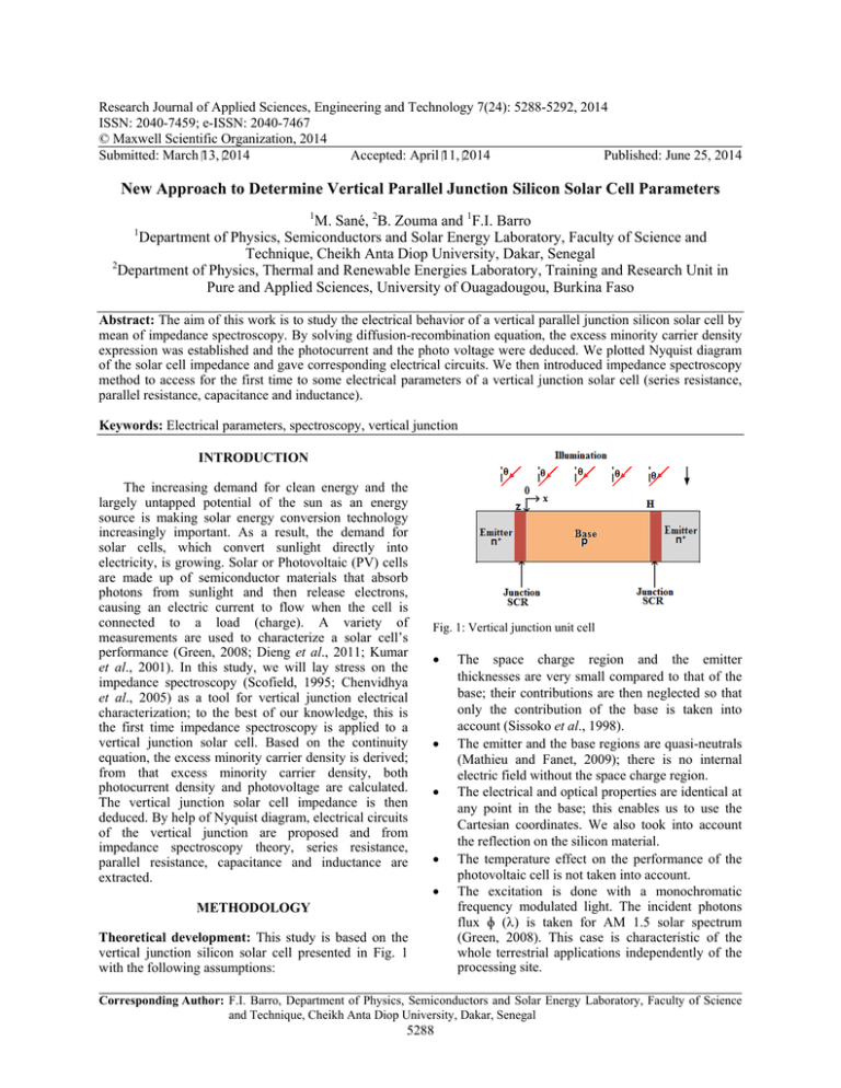
Fig. 1: Vertical junction unit cell
•
•
•
•
•
METHODOLOGY
Theoretical development: This study is based on the
vertical junction silicon solar cell presented in Fig. 1
with the following assumptions:
The space charge region and the emitter
thicknesses are very small compared to that of the
base; their contributions are then neglected so that
only the contribution of the base is taken into
account (Sissoko et al., 1998).
The emitter and the base regions are quasi-neutrals
(Mathieu and Fanet, 2009); there is no internal
electric field without the space charge region.
The electrical and optical properties are identical at
any point in the base; this enables us to use the
Cartesian coordinates. We also took into account
the reflection on the silicon material.
The temperature effect on the performance of the
photovoltaic cell is not taken into account.
The excitation is done with a monochromatic
frequency modulated light. The incident photons
flux ɸ (λ) is taken for AM 1.5 solar spectrum
(Green, 2008). This case is characteristic of the
whole terrestrial applications independently of the
processing site.
Corresponding Author: F.I. Barro, Department of Physics, Semiconductors and Solar Energy Laboratory, Faculty of Science
and Technique, Cheikh Anta Diop University, Dakar, Senegal
5288
Res. J. Appl. Sci. Eng. Technol., 7(24): 5288-5292, 2014
Excess minority carrier density: Taking into account
generation, recombination and diffusion phenomena in
the base, the equation governing the variation of the
minority carriers density δ (x, y, z, t) under frequency
modulation (Dieng et al., 2011) is:
∂ 2 δ ( x, θ , t ) δ ( x, θ , t )
−
=
D(ω ) ⋅
τ
∂x 2
∂δ ( x, θ , t )
− G ( z, θ , t ) +
∂t
•
2
(3)
x
ω
θ
z
λ
(9)
q is the elementary charge.
The factor 2 results from the two junctions around
the base and the fact that they are connected in a
parallel manner.
(10)
With V T the thermal voltage, Nb the base doping
density and n 0 the intrinsic carrier density.
(5)
Impedance: The vertical junction solar cell’s
impedance may be defined by Kumar et al. (2001) and
Dieng et al. (2011):
Z (ω , θ , z , Sf , λ ) =
V ph (ω , θ , z , Sf , λ )
J ph (ω , θ , z , Sf , λ )
(11)
The corresponding Nyquist diagram i.e., the
representation of imaginary part of the complex
function Z (ω, θ, z, Sf, λ) versus its real part (Kumar
et al., 2001; Chenvidhya et al., 2003; Chenvidhya et al.,
2005):
Im(Z (ω , θ , z, Sf , λ )) = f (Re(Z (ω , θ , z, Sf , λ )))
(12)
RESULTS AND DISCUSSION
(6)
Coefficients A and B is determined through the
following boundary conditions (Dieng et al., 2011):
At the junction (x = 0):
∂δ ( x, ω ,θ )
∂x
x =0
Nb
VPh = VT ⋅ ln 1 + 2 ⋅ δ (0 )
n0
The solution of this equation is in the form:
•
J Ph = 2 ⋅ q ⋅ D(ω ) ⋅
(4)
If we replace Eq. (2) into (1), the temporal part is
eliminated and we obtain:
x
x
+ B sinh
δ (x, ω , θ , z, Sf , λ ) = A cosh
L
(
ω
)
L(ω )
L(ω ) 2
+
⋅ α (λ )(1 − R(λ )) ⋅ φ (λ ) ⋅
D(ω )
exp(α (λ ) ⋅ z ) ⋅ cos(θ )
(8)
Photo voltage: According to the Boltzmann’s relation,
the photo voltage is given by Sze and Ng. Kwok (2007)
and Hu (2010):
= The base depth along x axis
= The angular frequency
= The incidence angle
= The base depth according to the vertical axis
= The illumination wavelength
g ( z, θ )
∂ 2 δ ( x ) δ ( x, θ , t )
−
=−
2
2
D(ω )
L(ω )
∂x
(7)
Photocurrent density: The main contribution to the
photocurrent Jph comes from diffusion; Jph can be
written in the form:
(2)
were,
g (z , θ , λ ) = α (λ ) (1 − R(λ ) )⋅ φ (λ ) ⋅
e x p−(α (λ ) ⋅ z ) ⋅ c o sθ()
∂δ (x, ω ,θ )
=0
H
∂x
x=
(1)
The excess minority carrier generation rate is given
by Dieng et al. (2011):
G ( z ,θ , λ , t ) = g ( z ,θ , λ ) exp(− jωt )
∂δ ( x, ω , θ )
= Sf ⋅ δ ( x, ω , θ ) x = 0
∂x
x =0
Sf is related to the carrier flow through the junction
(Diallo et al., 2008).
At the middle of the base (x = H/2):
D(ω ) ⋅
D (ω) and τ are, respectively the excess minority
carrier diffusion coefficient and lifetime.
The excess minority carrier density can be written as:
δ (x, t ) = δ (x ) exp(− jωt )
D(ω ) ⋅
We plotted in Fig. 2a and 3a the Nyquist diagram
of the vertical junction impedance; the obtained curves
are semi-circles of two types: positive one and negative
one depending on incidence angle value. For the
negative one (Fig. 2a) the parallel vertical junction
5289
Res. J. Appl. Sci. Eng. Technol., 7(24): 5288-5292, 2014
(a)
(b)
Fig. 2: (a) Nyquist diagram, (b) electrical circuit of solar cell for capacitive effects
Sf: 3.103 cm/sec; H: 0.03 cm; Lo: 0.02 cm; z: 0.0001 cm; Do: 26 cm²/sec; λ: 0.5 µm
(a)
(b)
Fig. 3: (a) Nyquist diagram, (b) electrical circuit of solar cell for inductive effects
Sf: 3.103 cm/sec; H: 0.03 cm; Lo: 0.02 cm; z: 0.0001 cm; Do: 26 cm²/sec; λ: 0.5 µm
5290
Res. J. Appl. Sci. Eng. Technol., 7(24): 5288-5292, 2014
behaves inductively contrary to the curve in Fig. 3a
where capacitance phenomenon predominates.
From these two behavior the vertical junction solar
cell can be represented by one of the electrical circuit
presented on Fig. 2b and 3b:
•
•
•
•
•
C is the total capacitance; C = C T + C D where C D is
the diffusion capacitance due to the diffusion of the
excess minority carrier density in the base and C T
is the transition capacitance due primarily to the
fixed atoms ionized in the space charge region.
Rsh models leakage currents existing at the edge of
the structure, the whole of the defects in the
vicinity of the space charge region (dislocation,
recombination centers) and in the base.
R D is the solar cell dynamic resistance, it indicate
the local behavior of the solar cell for a given
operating conditions.
Rs is the series resistance related to material
resistivity and metallization grid.
L is related to the inductive behavior of the cell; it
comes from the frequency effects through low
resistances particularly the quasi-neutrals regions
and metallization.
Fig. 4: Nyquist diagram with the particular points
Sf: 3.103 cm/sec; H: 0.03 cm; Lo: 0.02 cm; z: 0.0001
cm; Do: 26 cm²/sec; λ: 0.5 µm; θ: 48.2°
From the equations above, several particular cases
can be considered according to the modulation
frequency on one hand and to the ratio of R D and Rsh:
•
Both capacitive and inductive effects play very
important role in determining solar cell parameters (like
under flashed irradiance and transient experiments) and
in switching circuits with power inverters.
Impedance spectroscopy technique: If we consider
for example the capacitive behavior the cell with the
associated electrical circuit of Fig. 2b, the impedance
Z is given by Rs in series with Zc parallel to Rp;
Rp = Rsh//R D , Zc = 1/ (jcω). For the circuit of Fig. 3b,
the following calculations remain valid if Zc is replaced
by Z L = jLω.
We then have:
1
1
Z = RS +
+
R p ZC
−1
(13)
If we replace Rp and Zc by their expressions and
after some calculations, we obtain:
Z = RS +
RD ⋅ RSh ⋅ (RD + RSh )
(RD + RSh )2 + (ω ⋅ RD ⋅ RSh ⋅ C ) 2
2
j ⋅ ω ⋅ (RD ⋅ RSh ) ⋅ C
−
2
(RD + RSh ) + (ω ⋅ RD ⋅ RSh ⋅ C ) 2
(14)
Z is a complex number which real part Re (Z) and
imaginary part Im (Z) are given by:
Re( Z ) = RS
+
RD ⋅ RSh ⋅ (RD + RSh )
(RD + RSh )2 + (ω ⋅ RD ⋅ RSh ⋅ C ) 2
If ω→0, the imaginary part Im (Z) of Z is null and
only the real part Re (Z) remains:
Re (Z) = Rs + R D ·Rsh/ (R D + Rsh)
The impedance is rewritten in the form:
Z = Rs + R D ·Rsh/ (R D + Rsh)
o
o
•
If Rsh>>R D we have Re (Z) = Rs + R D and the
impedance Z is reduced to: Z = Rs + R D
If Rsh<<R D then one has Re (Z) = Rs + Rsh and
thus Z = Rs + Rsh
If ω→∞ the imaginary part Im (Z) of Z is also null
and we have: Re (Z) = Rs
The impedance can then is measured in the form:
Z = Rs independently of the ratio of Rsh and R D .
Taking into consideration these calculations, if we
return to the Nyquist diagram itself, we can associate
some particular points depending on the modulation
frequency (Dieng et al., 2011) as presented in Fig. 4.
The Nyquist diagram corresponds to a semi-circle
of radius Rp/2 and center (Rp/2+Rs, 0). A correspond
to low modulation frequency (ω→0) and C to higher
modulation frequencies (ω→∞). That is, some electrical
parameters can be determined the mean of the
technique described above.
Appling the impedance spectroscopy, we obtain
(Table 1).
To determine the associated capacitance, let us
consider the following equation obtained thanks to the
cut-off frequency:
τ C = Rp ⋅ C =
(15)
5291
2π
ωC
(16)
Res. J. Appl. Sci. Eng. Technol., 7(24): 5288-5292, 2014
Table 1: Series and parallel resistances capacitive behavior
6,7318.10-3
Rs (Ω.cm2)
2
1,254.103
Rp (Ω.cm )
Table 2: Series and parallel resistances inductive behavior
4,2225.10-3
Rs (Ω.cm2)
2,508.103
Rp (Ω.cm2)
That leads to C = 5,011.10-8 µF.
In the case of an inductive behavior, we have
(Table 2).
The associated inductance is deduced from Eq. (17):
τ L = Rp ⋅ L =
2π
ωc
(17)
This leads to L = 2,505/108 µH.
CONCLUSION
Based on an ac-equivalent circuit of a parallel
vertical junction solar cell, an expression of the
impedance has been established. From Nyquist
diagram, we presented two electrical circuits of the
solar cell. The impedance spectroscopy technique is
then applied to extract for the first time the vertical
junction electrical parameters.
REFERENCES
Chenvidhya, D., K. Kirtikara and C. Jivacate, 2003. A
new characterization method for solar cell dynamic
impedance. Sol. Energ. Mat. Sol. C., 80:
459-464.
Chenvidhya, D., D. Kirtikara and C. Jivacate, 2005. PV
module dynamic impedance and its voltage and
frequency dependencies. Sol. Energ. Mat. Sol.
C., 86(2) pp: 243-251.
Diallo, H.L., A. Wereme, A.S. Maiga and G. Sissoko,
2008. New approach of both junction and back
surface recombination velocities in a 3D modelling
study of a polycrystalline silicon solar cell. Eur.
Phys. J-Appl. Phys., 42: 203-211.
Dieng, A., I. Zerbo, M. Wade, A.S. Maiga and
G. Sissoko, 2011. Three-dimensional study of a
polycrystalline silicon solar cell: The influence of
the applied magnetic field on the electrical
parameters. Semicond. Sci. Tech., 26(095023): 9.
Green, M.A., 2008. Self-consistent optical parameters
of intrinsic silicon at 300K including temperature
coefficients. Sol. Energ. Mat. Sol. C., 92:
1305-1310.
Hu, C.C., 2010. Modern Semiconductor Devices for
Integrated Circuits. Pearson/Prentice Hall, New
Jersey.
Kumar, R.A., M.S. Suresh and J. Nagaraju, 2001.
Measurement of AC parameters of gallium
arsenide (GaAs/Ge) solar cell by impedance
spectroscopy. IEEE T. Electron. Dev., 48(9):
2177-2179.
Mathieu, H. and H. Fanet, 2009. Physique des SemiConducteurs et Des Composants Electroniques. 6th
Edn., Dunod, Paris.
Scofield, J.H., 1995. Effects of series resistance and
inductance on solar cell admittance measurements.
Sol. Energ. Mat. Sol. C., 37(2): 217-233.
Sissoko, G., E. Nanema, A. Correa, M. Adj,
A.L. Ndiaye and M.N. Diarra, 1998.
Recombination parameters measurement in double
sided surface field solar cell. Renew. Energ., 3 :
1856-1859.
Sze, S.M. and K. Ng. Kwok, 2007. Physics of
Semiconductors Devices. Wiley, New York.
5292


